There are many applications for Micro Electro-Mechanical Systems (MEMS) within the automotive, medical, biochemical and aeronautic industries. To achieve high yield and reliability at a low production cost, an increasingly important measurement is wafer-level MEMS testing before packaging.
Both changing environmental conditions (for example, pressure, light, temperature and fluids) and intrinsic parameters (for example, resonance frequencies and displacements) can cause a MEMS device to respond differently. For this reason, measuring the response is crucial to the dynamic design of new sensors. This article describes the use of a semiautomatic probe station equipped with a scanning laser-Doppler vibrometer for characterizing the dynamic response of membranes.
Step-and-Repeat MEMS Wafer Testing
When carried out manually, dynamic testing of a MEMS wafer covered with an array of micro-membranes is extremely time-consuming as only one device can be tested at a time. A combination of a semiautomatic probe station used to position the wafer and a laser-Doppler vibrometer used to perform the dynamic test on each device improves the throughput significantly.
Software is used to control the entire process, which steps the wafer and initiates a measurement. The whole system comprises the Polytec MSA-400 Micro System Analyzer hardware running the Scanning Vibrometer Software, a SUSS PA200 Probe Station equipped with the MSA-400 Measurement Microscope Head, the probe station controller hardware, and the SUSS ProberBench™ Operating System.
First, the locations of the structures on the wafer are programmed by aligning the wafer. Using this information, the software can then generate a wafer map. Following on from this, the measurement parameters for the vibration characterization of the membrane need to be defined. A grid consisting of 6 to 9 measurement points as shown in Figure 1 is fitted to a single membrane structure for the membrane array MEMS device. Once these steps have been completed, the step-and-repeat measurements on the MEMS device can be initiated by the software.
The system steps to each membrane on the wafer from the first to the last as originally programmed. A scanning vibrometer measurement is performed on each membrane within 2 to 3 seconds (as shown in Figure 2 and Figure 1, bottom). This is then saved alongside the device ID. This means that the full wafer map is measured and ensures the availability of frequency spectra along with deflection shapes of all devices (Figure 3).
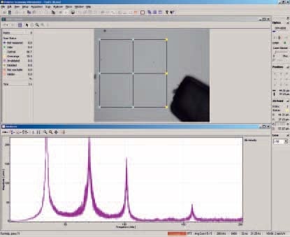
Figure 1: Measurement grid (top) and frequency spectrum (bottom) of the device displayed in the Polytec Scanning Vibrometer Software.
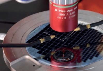
Figure 2: Scanning laser-Doppler vibrometer measurement of a single MEMS membrane on the wafer.
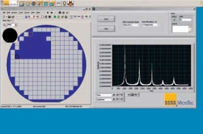
Figure 3: Wafer testing process and vibration signal displayed in the SUSS ProberBench™ Software.
SUSS PA200
Semiautomatic Probe System for Direct MEMS Testing at Wafer-Level
An accurate and flexible semiautomatic test solution for wafers is the SUSS PA200 for substrates up to 200 mm. This semiautomatic probe system is good for failure analysis, high-frequency measurements, optomechanical engineering, and MEMS tests.
Reliable probing is ensured with the PA200 along with precise measurements on decreasing pad and feature sizes down to the sub-micron range. Due to its modular design concept, the PA200 can be upgraded from a simple manual microscope stage to a fully programmable microscope with high magnification. There are various accessories available, including laser cutters, specially designed chucks for HF measurements and probe card adapters. The unique SUSS ProberBench™ operating system controls the PA200.
This consists of an electronics rack, a full prober control joystick controller and a graphical user interface. ProberBench™ interfaces with test equipment and software from all leading vendors. More information can be found on www.suss.com.
Polytec Micro System Analyzer
For Measurements of 3-D MEMS Dynamics and Topography
The Micro System Analyzer series was developed to analyze and visualize structural vibrations and surface topography in microstructures such as MEMS devices. The MSA is easily mounted onto manual or fully automated probe stations for wafer-level testing. It is an all-in-one combination of technologies fully integrating a microscope with scanning laser-Doppler vibrometry, stroboscopic video microscopy, and white light interferometry to clarify real microstructural response and topography.
Accurate 3D dynamic and static response data are incorporated into the MEMS design and test cycle, which simplifies troubleshooting, enhances and shortens design cycles, improves yield and performance, and reduces product cost.
The new MSA-500 has an added features compared to the MSA-400. These include an Autofocus and Geometry Scan that widens the vertical measurement range and allows a complete 3D view of the vibrations.

This information has been sourced, reviewed and adapted from materials provided by Polytec.
For more information on this source, please visit Polytec.