Published in the journal nanomaterials, a team of researchers has developed a small plasmonic pressure sensor that could help to advance nanophotonic devices.

Image Credit: narong sutinkham/Shutterstock.com
Surface plasmon polaritons (SPP's) are electromagnetic (EM) waves that mediate light-matter interactions between metal nanoparticles (MNPs) and a dielectric device, which is polarised when exposed to an applied electric field. These waves travel along the dielectric-metal border and form collective oscillations of photons and electrons at resonant wavelengths.
SPPs’ exceptional optical properties make them suitable for applications in numerous areas, particularly nanophotonics.
A MIM (metal-insulator-metal)-based plasmonic pressure sensor is an optical element that is capable of undergoing exerted pressure and converting it into optical or electrical signals.
To improve integrated optical circuits (IOC) compatibility with the pressure sensor, its size has to be reduced. Although extensive research has been conducted on this topic, complicated fabrication processes are often involved. On top of this, researchers are faced with improving sensitivity due to advancements in current pressure sensor applications.
In this article, a plasmonic pressure sensor was constructed at the nanoscale with a significant increase in sensitivity compared to previous efforts. These results, as well as the innovative sensors ease of design, are indicative of its great potential for advancing nanophoptonic devices.
Methodology
Figure 1a, b depicts the schematics of the sensor. The golden and white parts in the figure depict silver (Ag) and air. In case an applied pressure F is given on the top of the Ag layer, it would bend downwards with deformation of d.
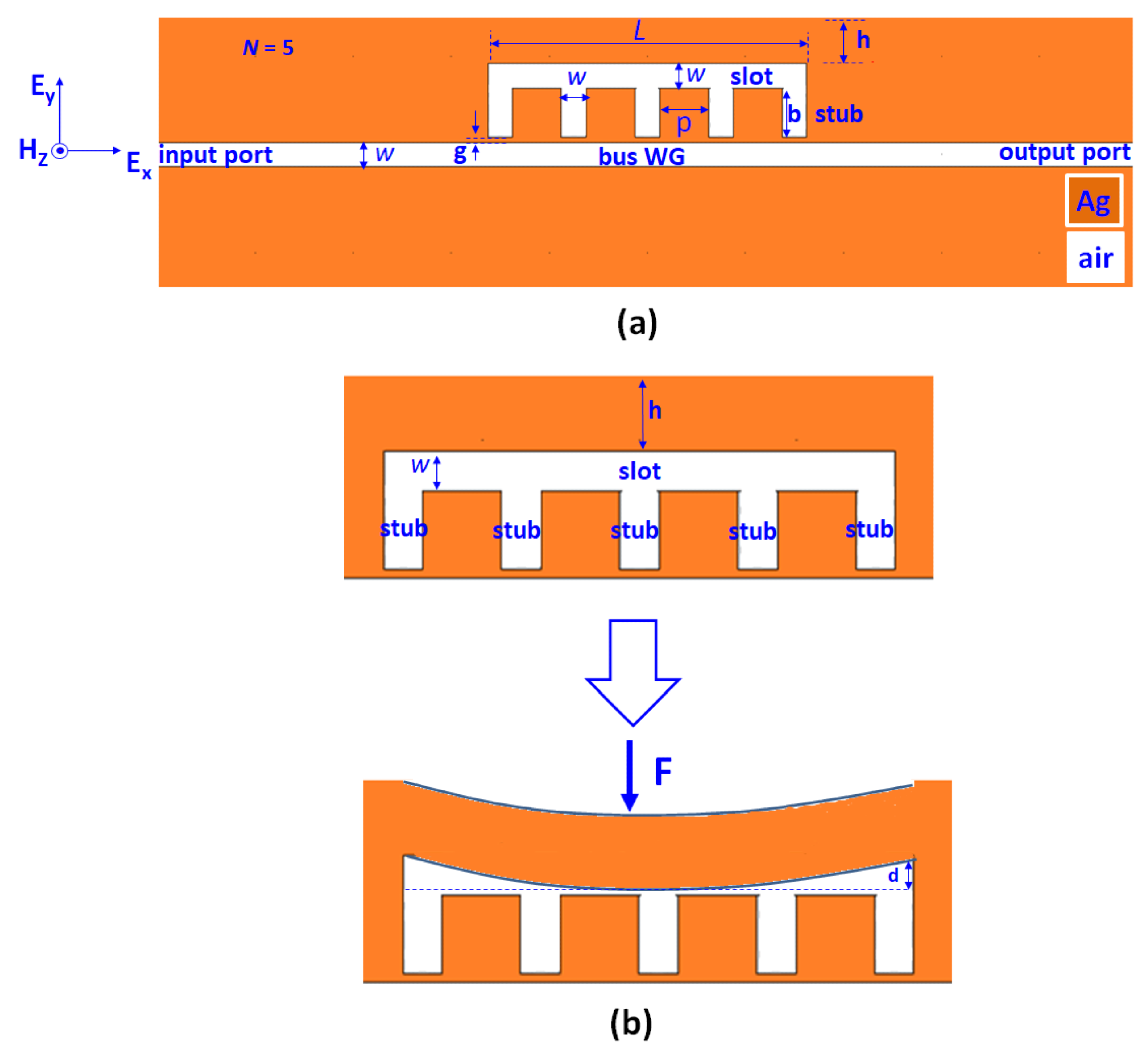
Figure 1. (a) Schematic diagram of the designed sensor. (b) Schematic diagram of an applied pressure F exerted on the Ag layer. Image Credit: Chao, et al., 2021
A TM-polarized incident light pairs with the fundamental SPP mode into the input port of the bus waveguide's (WG), and the transmission power attains the output port.
This research uses Ag as the plasmonic metal as it is cost-effective, and its EM wave response has the least imaginary part of relative permittivity within the near-infrared level resulting in low power consumption. The transmittance spectrum and EM wave distributions were stimulated with FEM-based COMSOL Multiphysics with ultrafine mesh sizes.
The transmittance spectrum for the developed structure without exerting pressure on the system is depicted in Figure 2.
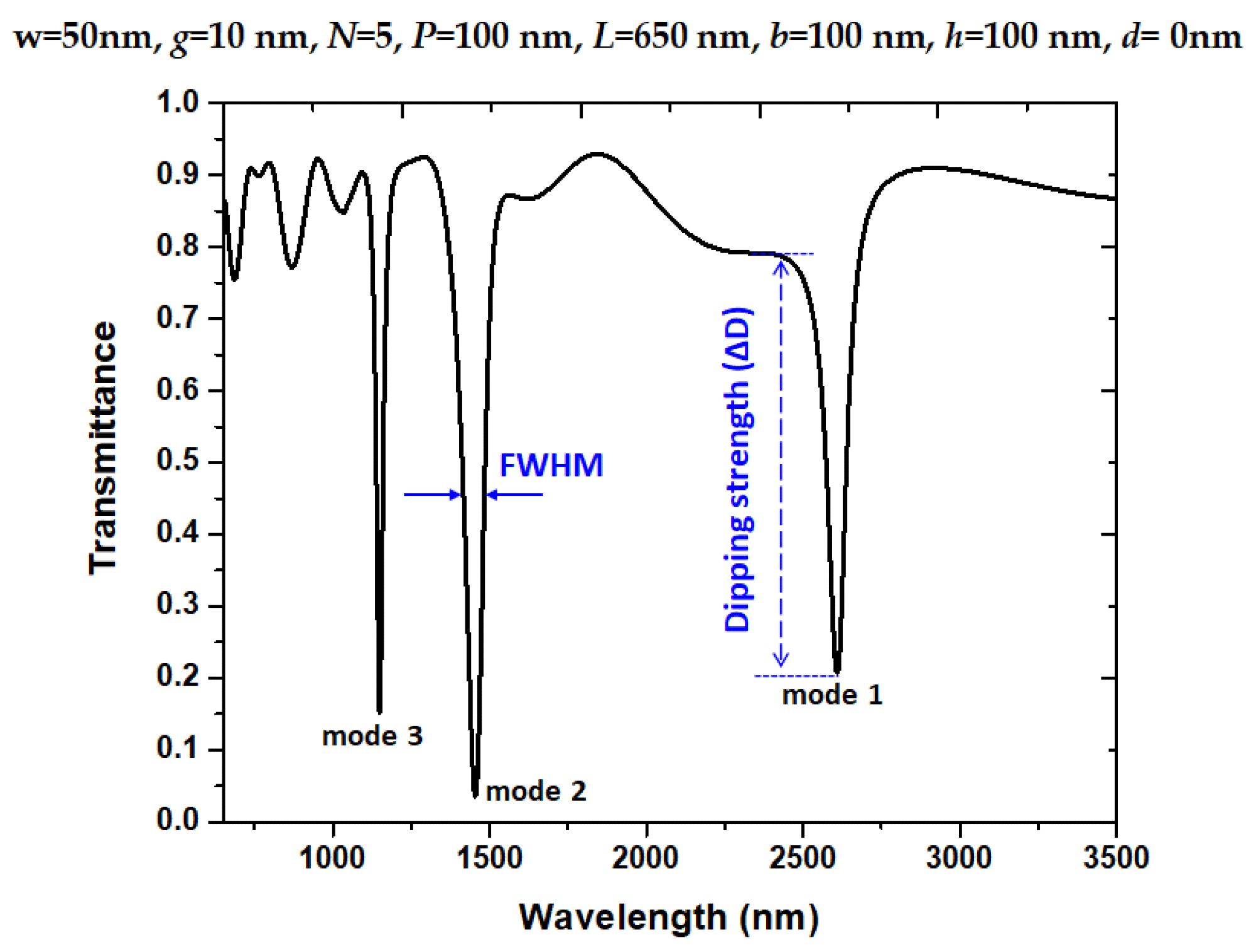
Figure 2. Transmittance spectrum for the designed structure without pressure on the system (i.e., d = 0 nm). Image Credit: Chao, et al., 2021
The advancements in nanofabrication enabled easy fabrication of the designed pressure sensor. The MIM waveguide comprising of a rectangular shape was achieved with stripping and ion beam lithography processes.
Results
The bus WG’s width was retained as w = 50 nm to ensure that the TM mode travels in bus WG. The resonator size of the developed sensor is compact and very smaller than earlier designs.
Table 1 compares the resonance wavelength (λres), dipping strength (∆D), FWHM, and QF of the structure at corresponding resonance modes. It was noted that the resonance dips in the developed sensor had a more profound ∆D, a higher QF, and a narrower FWHM. Moreover, the transmission loss has the least influence on sensing performance as the designed device has fewer transmission loss values at resonance modes.
Table 1. Comparison of λres, FWHM, ΔD, and QF of the designed structures at corresponding resonance modes. Source: Chao, et al., 2021
| |
Mode 1 |
Mode 2 |
Mode 3 |
| λres (nm) |
2608 |
1454 |
1149 |
| FWHM (nm) |
60.00 |
50.00 |
40.00 |
| ΔD (%) |
58.37 |
92.16 |
90.24 |
| QF |
43.47 |
29.08 |
36.35 |
The normalized magnetic field intensity and electric field intensity at the corresponding resonance modes is illustrated in Figure 3.
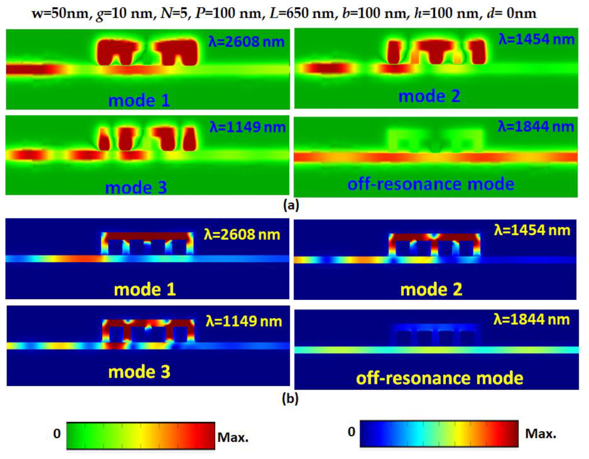
Figure 3. Normalized (a) magnetic field intensity and (b) electric field intensity at the corresponding resonance modes and one of the off-resonance modes. Image Credit: Chao, et al., 2021
The transmittance spectra of the developed structure with a variation of d from 0 to 10 nm is shown in Figure 4.
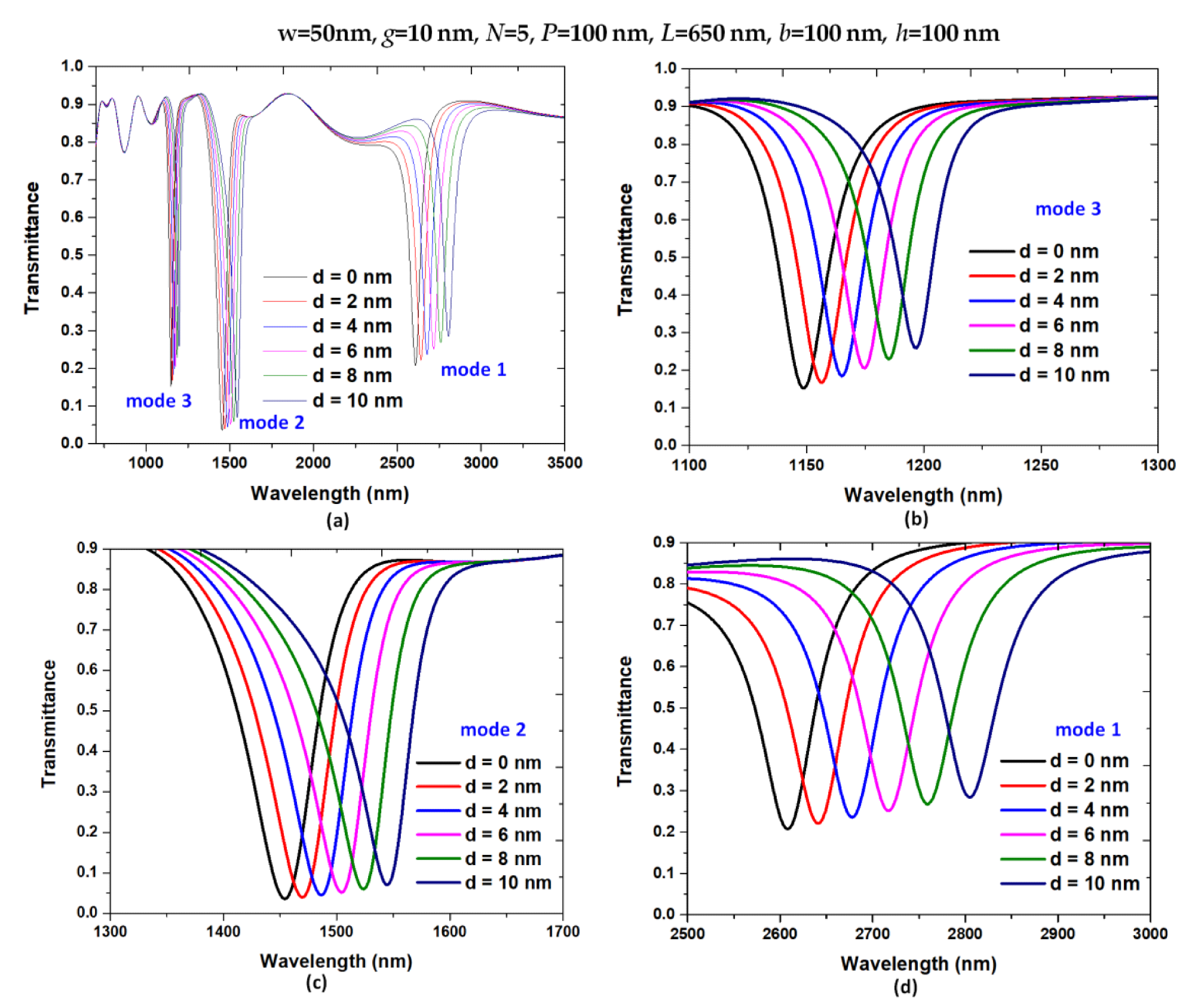
Figure 4. Transmittance spectra of the designed structure with a variation of d from 0 to 10 nm with an interval of 2 nm in the wavelength of (a) 700–3500 nm for modes 1–3, (b) 1100–1300 nm for mode 3, (c) 1300–1700 nm for mode 2, and (d) 2500–3000 nm for mode 1, respectively. Image Credit: Chao, et al., 2021
A pressure influence on the upper horizontal slot indicates deformation. Figure 5 illustrates the linear relationship between λres and d.
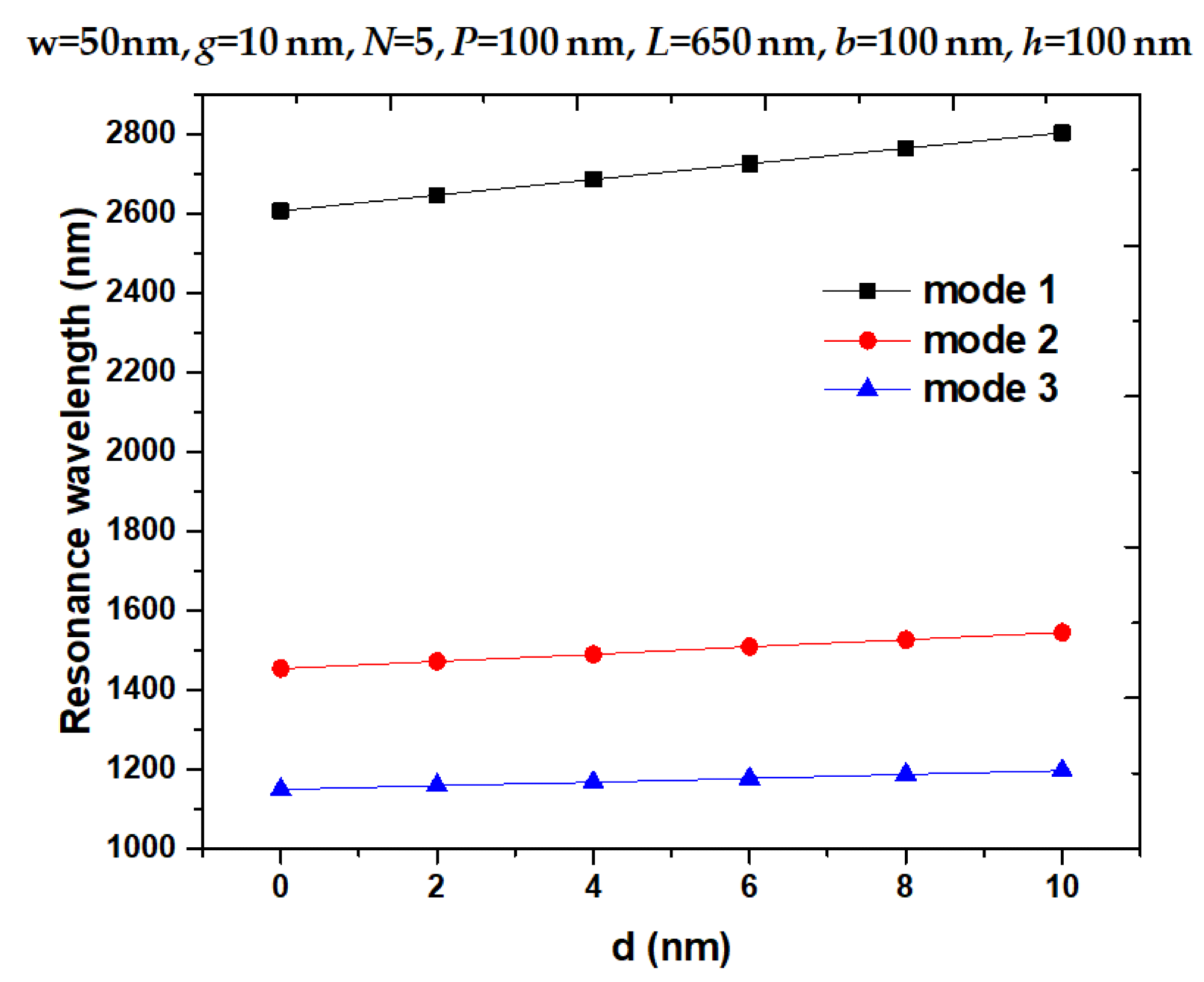
Figure 5. Resonance wavelength versus variation of d from 0 to 10 nm with an interval of 2 nm. Image Credit: Chao, et al., 2021
The transmittance spectrum of the designed structure when the deformation d in various nm is illustrated in Figure 6.
The transmittance dip would redshift as d increases and fade when d = 50 nm also, the FWHM enlarges and the dipping strength decreases with an increase in d. This results in asymmetricity impacting the linearity of the resonant wavelength vs. d.
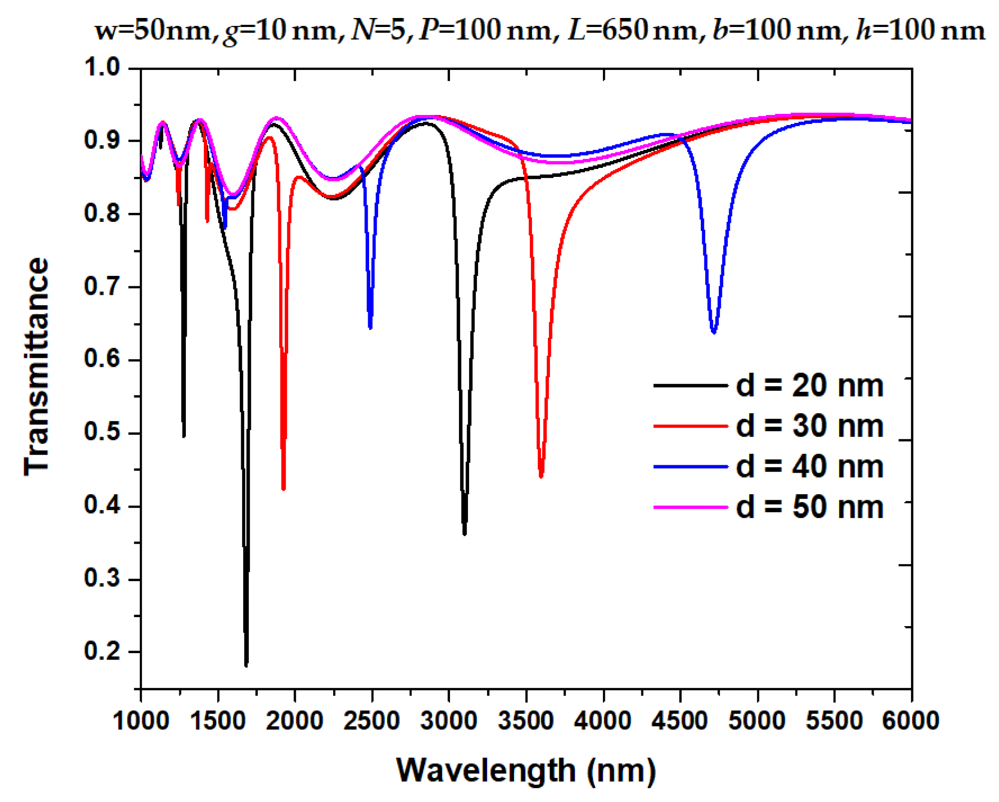
Figure 6. Transmittance spectrum of the proposed structure when deformation d = 20 nm, 30 nm, 40 nm, and 50 nm, respectively. Image Credit: Chao, et al., 2021
The observations show that the structural parameters have a major impact on the sensing performance of developed plasmonic pressure sensors (see Figure 7).
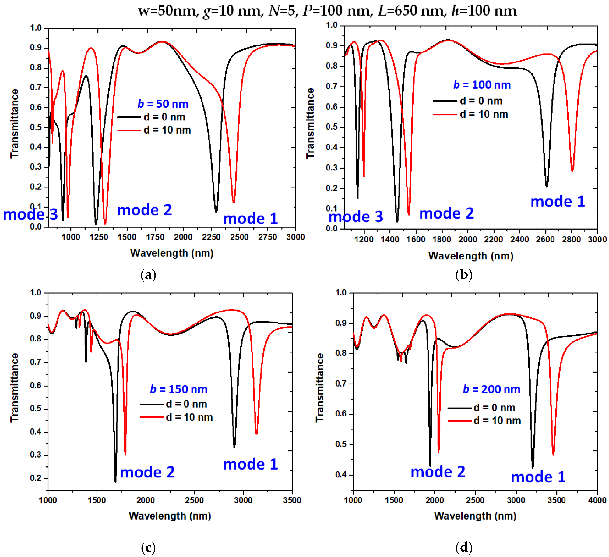
Figure 7. Transmittance spectra of the designed structure with variation of the height of stubs (b), (a) b = 50 nm, (b) b = 100 nm, (c) b = 150 nm, and (d) b = 200 nm, respectively. Image Credit: Chao, et al., 2021
The resonance wavelength shift (∆λres) and sensitivity S(nm/MPa) were compared and listed in Table 2.
Table 2. Comparison of [∆λres(nm), S(nm/MPa)] of the designed structure for b = 50, 100, 150, and 200 nm. Source: Chao, et al., 2021
| (∆λres, S) |
Mode 1 |
Mode 2 |
Mode 3 |
| b = 50 nm |
(155, 18.45) |
(80, 9.25) |
(45, 5.34) |
| b = 100 nm |
(197, 23.44) |
(91, 10.82) |
(48, 5.71) |
| b = 150 nm |
(227, 27.01) |
(99, 11.78) |
|
| b = 200 nm |
(254, 30.23) |
(105, 12.50) |
|
The transmittance spectra of the developed structure containing variation in the number of stubs (N), when N = 3, 5, 7, and 9 are shown in Figure 8.
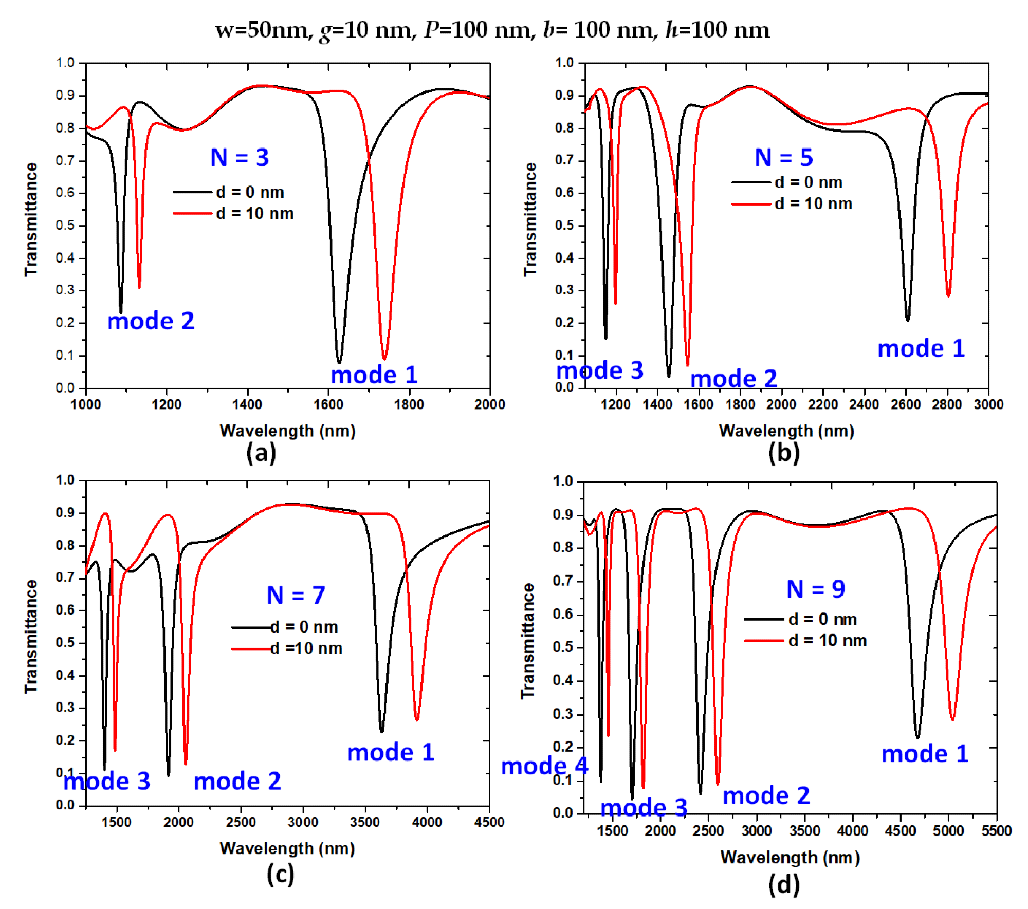
Figure 8. Transmittance spectra of the designed structure with a variation of the number of stubs (N), (a) N = 3, (b) N = 5, (c) N = 7, and (d) N = 9, respectively. Image Credit: Chao, et al., 2021
Table 3 lists the (∆λres, S) of the developed structure for N = 3, 5, 7, and 9.
Table 3. Comparison of (∆λres(nm), S(nm/MPa)) of the designed structure for N = 3, 5, 7, and 9. Source: Chao, et al., 2021
| (∆λres, S) |
Mode 1 |
Mode 2 |
Mode 3 |
Mode 4 |
| N = 3 |
(113, 11.31) |
(46, 4.61) |
|
|
| N = 5 |
(197, 23.44) |
(91, 10.82) |
(48, 5.71) |
|
| N = 7 |
(283, 153.67) |
(139, 73.85) |
(85, 46.16) |
|
| N = 9 |
(364, 592.44) |
(181, 294.60) |
(116, 188.80) |
(74, 120.44) |
Table 4 shows the comparisons between the developed plasmonic pressure sensor with the published designs. The sensor shows increased sensitivity (≈23.32 times).
Table 4. Comparison of the designed plasmonic pressure sensor with the published designs. Source: Chao, et al., 2021
Reference/
Year |
Structure/
Size |
Max. S
(nm/MPa) |
Max.
∆λres (nm) |
Operating
Wavelength |
| [82]/2008 |
long PM-PCF/58.4 cm |
3.42 |
5.30 |
1550 nm < λ <
1555 nm |
| [37]/2012 |
nanoring resonator/1500 ×
1500 μm2 |
1.47 |
- |
1602.3 nm < λ <
1602.9 nm |
| [80]/2016 |
π-shaped resonator/400 ×
150 nm2 |
8.5 |
80.00 |
600 nm < λ <
1800 nm |
| [55]/2018 |
double square resonator/
700 ×
500 nm2 |
16.5 |
103.00 |
350 nm < λ <
1350 nm |
| [46]/2020 |
thin-walled oval cylinder/
6 × 17 × 0.5 mm3 |
1.198 |
- |
1549 nm < λ <
1558 nm |
| [54]/2021 |
34 Ag nanorods in slots/
800 × 230 nm2 |
25.4 |
92.93 |
1400 nm < λ <
2200 nm |
| This work |
one slot and nine stubs/
1250 × 150 nm2 |
592.44 |
364.00 |
1000 nm < λ <
5500 nm |
Here, a compact and simple plasmonic pressure sensor structure featuring a bus waveguide and a resonator with a horizontal slot and numerous stubs was developed. This sensor can be applied for small-scale ultrahigh-pressure sensitivity.
The observations show that the resonance wavelength redshift comprises a linear relationship with the resonator’s deformation. The sensor developed possesses an ultra-high sensitivity of 592.44 nm/MPa having the highest value and achieving 23.32 times more sensitivity.
Continue reading: Using Surface Enhanced Raman Spectroscopy for Molecular Sensing.
Journal Reference:
Chao, C.-T. C., Chau, Y.-F. C., Chen, S.-H., Huang, H. J., Lim, C. M., Kooh, M. R. R., Thotagamuge, R., Chiang, H.-P. (2021) Ultrahigh Sensitivity of a Plasmonic Pressure Sensor with a Compact Size. Nanomaterials, 11(11), p. 3147. Available online: https://www.mdpi.com/2079-4991/11/11/3147/htm.
References and Further Reading
- Zhang, J., et al. (2012) Surface plasmon polaritons: Physics and applications. Journal of Physics D: Applied Physics, 45, p. 113001. doi.org/10.1088/0022-3727/45/11/113001.
- Han, Z & Bozhevolnyi, S I (2012) Radiation guiding with surface plasmon polaritons. Reports on Progress in Physics, 76, p. 016402. doi.org/10.1088/0034-4885/76/1/016402.
- Hsieh, L.-Z., et al. (2016) Tunable plasmonic resonance arising from broken-symmetric silver nanobeads with dielectric cores. Optics Communications, 370, pp. 85–90 doi.org/10.1016/j.optcom.2016.03.009.
- Ho, Y. Z., et al. (2012) Tunable plasmonic resonance arising from broken-symmetric silver nanobeads with dielectric cores. Journal of Optics, 14, p. 114010. doi.org/10.1088/2040-8978/14/11/114010.
- Chau, Y-F & Jiang, Z-H (2011) Plasmonics Effects of Nanometal Embedded in a Dielectric Substrate. Plasmonics, 6, pp. 581–589. doi.org/10.1007/s11468-011-9238-z.
- Qiao, L., et al. (2019) Study on the Fano resonance of coupling M-type cavity based on surface plasmon polaritons. Optics Communications, 433, pp. 144–149. doi.org/10.1016/j.optcom.2018.09.055.
- Al Mahmud, R., et al. (2021) Plasmonic Refractive Index Sensor Based on Ring-Type Pentagonal Resonator with High Sensitivity. Plasmonics, 16, pp. 873–880. doi.org/10.1007/s11468-020-01357-7.
- Kravets, V. G., et al. (2018) Plasmonic Surface Lattice Resonances: A Review of Properties and Applications. Chemical Reviews, 118, pp. 5912–5951. doi.org/10.1021/acs.chemrev.8b00243.
- Ahmadivand, A., et al. (2020) Terahertz plasmonics: The rise of toroidal metadevices towards immunobiosensings. Materials Today, 32, pp. 108–130. doi.org/10.1016/j.mattod.2019.08.002.
- Chou Chau, Y.-F., et al. (2019) Plasmonic perfect absorber based on metal nanorod arrays connected with veins. Results in Physics, 15, p. 102567. doi.org/10.1016/j.rinp.2019.102567.
- Chau, Y. F., et al. (2010) A New Type of Optical Antenna: Plasmonics Nanoshell Bowtie Antenna with Dielectric Hole. Journal of Electromagnetic Waves and Applications, 24, pp. 1621–1632. doi.org/10.1163/156939310792149588.
- Chen, W. T., et al. (2010) Electromagnetic energy vortex associated with sub-wavelength plasmonic Taiji marks. Optics Express, 18, pp. 19665–19671. doi.org/10.1364/OE.18.019665.
- Chau, Y.-F., et al. (2004) Coupling technique for efficient interfacing between silica waveguides and planar photonic crystal circuits. Applied Optics, 43, pp. 6656–6663. doi.org/10.1364/AO.43.006656.
- Sung, M.-J., et al. (2010) Surface plasmon resonance in a hexagonal nanostructure formed by seven core shell nanocylinders. Applied Optics, 49, pp. 920–926. doi.org/10.1364/AO.49.000920.
- Chau, Y.-F. C., et al. (2007) Three-dimensional analysis of silver nano-particles doping effects on super resolution near-field structure. Optics Communications, 269, pp. 389–394. doi.org/10.1016/j.optcom.2006.08.004.
- Tian, M., et al. (2012) Plasmonic Bragg reflectors based on metal-embedded MIM structure. Optics Communications, 285, pp. 5122–5127. doi.org/10.1016/j.optcom.2012.07.072.
- Shi, L., et al. (2019) Plasmonic filter with highly selective wavelength in a fixed dimension based on the loaded rectangular ring cavity. Optics Communications, 439, pp. 125–128. doi.org/10.1016/j.optcom.2019.01.058.
- Amoosoltani, N., et al. (2021) Double-Ring Resonator Plasmonic Refractive Index Sensor Utilizing Dual-Band Unidirectional Reflectionless Propagation Effect. Plasmonics, 16, pp. 1277–1285. doi.org/10.1007/s11468-021-01395-9.
- Chau, Y.-F., et al. (2010) Enhanced surface plasmon resonance based on the silver nanoshells connected by the nanobars. Optics Express, 18, pp. 3510–3518. doi.org/10.1364/OE.18.003510.
- Chou Chao, C.-T., et al. (2020) Highly Sensitive and Tunable Plasmonic Sensor Based on a Nanoring Resonator with Silver Nanorods. Nanomaterials, 10, p. 1399. doi.org/10.3390/nano10071399.
- Chou Chau, Y.-F., et al. (2021) Significantly enhanced coupling effect and gap plasmon resonance in a MIM-cavity based sensing structure. Scientific Reports, 11, p. 18515. doi.org/10.1038/s41598-021-98001-z.
- Shen, L., et al. (2007) 50/50 beam splitter using a one-dimensional metal photonic crystal with parabolalike dispersion. Applied Physics Letters, 90, p. 251909. doi.org/10.1063/1.2750385.
- Shen, L., et al. (2008) Effect of internal period on the optical dispersion of indefinite-medium materials. Physical Review B, 77, p. 205124. doi.org/10.1103/PhysRevB.77.205124.
- Karimi, Y., et al. (2021) All-optical plasmonic switches based on Fano resonance in an X-shaped resonator coupled to parallel stubs for telecommunication applications. Optik, 243, p. 167424. doi.org/10.1016/j.ijleo.2021.167424.
- Chou Chau, Y. F., et al. (2020) Ultrawide Bandgap and High Sensitivity of a Plasmonic Metal-Insulator-Metal Waveguide Filter with Cavity and Baffles. Nanomaterials, 10, p. 2030. doi.org/10.3390/nano10102030.
- Guo, Y., et al. (2011) A plasmonic splitter based on slot cavity. Optics Express, 19, 13831–13838. doi.org/10.1364/OE.19.013831.
- Liu, X., et al. (2019) All-Metal Resonant Metamaterials for One-, Two-, Three-Band Perfect Light Absorbers and Sensors. Plasmonics, 14, pp. 967–971. doi.org/10.1007/s11468-018-0881-5.
- Yuan, L., et al. (2021) Ultra-narrow-band Infrared Absorbers Based on Surface Plasmon Resonance. Plasmonics, 16, pp. 1165–1174. doi.org/10.1007/s11468-021-01384-y.
- Zhu, L., et al. (2020) Ultra-Broadband Absorber Based on Metal-Insulator-Metal Four-Headed Arrow Nanostructure. Plasmonics, 15, pp. 2153–2159. doi.org/10.1007/s11468-020-01244-1.
- Qi, Y., et al. (2019) Theoretical study of a multichannel plasmonic waveguide notch filter with double-sided nanodisk and two slot cavities. Results in Physics, 14, p. 102506. doi.org/10.1016/j.rinp.2019.102506.
- Lin, J-M & Chau, Y-F (1995) Radome slope compensation using multiple-model Kalman filters. Journal of Guidance, Control, and Dynamics, 18, pp. 637–640. doi.org/10.2514/3.21438.
- Zhou, C., et al. (2021) Tunable Multiple Fano Resonances and Stable Plasmonic Band-Stop Filter Based on a Metal-Insulator-Metal Waveguide. Plasmonics, 16, pp. 1735–1743. doi.org/10.1007/s11468-021-01437-2.
- Chou Chau, Y.-F., et al. (2019) Fabrication and Characterization of a Metallic–Dielectric Nanorod Array by Nanosphere Lithography for Plasmonic Sensing Application. Application. Nanomaterials, 9, p. 1691. doi.org/10.3390/nano9121691.
- Su, C & Zhu, J (2021) Novel SPR Sensor Based on MIM-based Waveguide and an Asymmetric Cross-shaped Resonator. Plasmonics, 16, pp. 769–775. doi.org/10.1007/s11468-020-01348-8.
- Topcu, G., et al. (2019) Colorimetric and plasmonic pressure sensors based on polyacrylamide/Au nanoparticles. Sensors and Actuators A: Physical, 295, pp. 503–511. doi.org/10.1016/j.sna.2019.06.038.
- Rajasekar, R., et al. (2019) Nano-Pressure and Temperature Sensor Based on Hexagonal Photonic Crystal Ring Resonator. Plasmonics, 14, pp. 3–15. doi.org/10.1007/s11468-018-0771-x.
- Zhao, X., et al. (2021) A nano-opto-mechanical pressure sensor via ring resonator. Optics Express, 20, pp. 8535–8542. doi.org/10.1364/OE.20.008535.
- Kazanskiy, N. L., et al. (2020) Plasmonic sensors based on Metal-insulator-metal waveguides for refractive index sensing applications: A brief review. Physica E: Low-dimensional Systems and Nanostructures, 117, p. 113798. doi.org/10.1016/j.physe.2019.113798.
- Chao, Y.-C., et al. (2009) Low voltage active pressure sensor based on polymer space-charge-limited transistor. Applied Physics Letters, 95, p. 253306. doi.org/10.1063/1.3266847.
- Yao, M., et al. (2018) Optical Fiber-Tip Sensors Based on In-Situ µ-Printed Polymer Suspended-Microbeams. Sensors, 18, p. 1825. doi.org/10.3390/s18061825.
- Liu, J., et al. (2018) Fiber-optic Fabry–Perot pressure sensor based on low-temperature co-fired ceramic technology for high-temperature applications. Applied Optics, 57, pp. 4211–4215. doi.org/10.1364/AO.57.004211.
- Donlagic, D., et al. (2005) All-fiber high-sensitivity pressure sensor with SiO2 diaphragm. Optics Letters, 30, pp. 2071–2073. doi.org/10.1364/OL.30.002071.
- Sander, C., et al. (1980) A monolithic capacitive pressure sensor with pulse-period output. In: Digest of Technical Papers, Proceedings of the 1980 IEEE International Solid-State Circuits Conference, San Francisco, CA, USA, 13–15 February 1980; IEEE: Piscataway, NJ, USA, pp. 78–79.
- Sarra, B & Ameur, Z (2018) Improved Sensitivity of 2D Photonic Crystal Mach–Zehnder Interferometer-Based Pressure Sensor. Plasmonics, 13, pp. 413–418. doi.org/10.1007/s11468-017-0525-1.
- Lee, B.H., et al. (2012) Interferometric Fiber Optic Sensors. Sensors, 12, pp. 2467–2486. doi.org/10.3390/s120302467.
- Hong-Kun, Z., et al. (2020) High sensitivity optical fiber pressure sensor based on thin-walled oval cylinder. Sensors and Actuators A Physical, 310, p. 112042. doi.org/10.1016/j.sna.2020.112042.
- Martín-Sánchez, C., et al. (2020) Plasmonic Sensing of Refractive Index and Density in Methanol–Ethanol Mixtures at High Pressure. Journal of Physical Chemistry C, 124, pp. 8978–8983. doi.org/10.1021/acs.jpcc.0c01419.
- Runowski, M., et al. (2019) Gold Nanorods as a High-pressure Sensor of Phase Transitions and Refractive-Index Gauge. Nanoscale, 11, pp.8718–8726. doi.org/10.1039/C9NR02792K.
- Chaudhary, V.S., et al. (2020) Hybrid dual core photonic crystal fiber as hydrostatic pressure sensor. Optik, 210, p. 164497. doi.org/10.1016/j.ijleo.2020.164497.
- Dinodiya, S & Bhargava, A (2021) A Comparative Analysis of Pressure Sensing Parameters for Two Dimensional Photonic Crystal Sensors Based on Si and GaAs. Silicon, pp. 1–8. doi.org/10.1007/s12633-021-01246-6.
- Mansouri, M., et al. (2021) Numerical Modeling of an Integrable and Tunable Plasmonic Pressure Sensor with Nanostructure Grating. Plasmonics, 16, pp. 27–36. doi.org/10.1007/s12633-021-01246-6.
- Wu, J., et al. (2016) A novel optical pressure sensor based on surface plasmon polariton resonator. Journal of Modern Optics, 63, pp. 219–223. doi.org/10.1080/09500340.2015.1073806.
- Yu, X., et al. (2018) Flexible Plasmonic Pressure Sensor Based on Layered Two-Dimensional Heterostructures. Journal of Lightwave Technology, 36, 5678–5684. doi.org/10.1109/JLT.2018.2877419.
- Tathfif, I., et al. (2021) Metal-insulator-metal waveguide-based optical pressure sensor embedded with arrays of silver nanorods. Optics Express, 29, pp. 32365–32376. doi.org/10.1364/OE.439974.
- Palizvan, P., et al. (2018) An Optical MIM Pressure Sensor Based on a Double Square Ring Resonator. Photonic Sensors, 8, pp. 242–247. doi.org/10.1007/s13320-018-0491-z.
- Chen, W -C., et al. (2016) Role of surface electromagnetic waves in metamaterial absorbers. Optics Express, 24, pp. 6783–6792. doi.org/10.1364/OE.24.006783.
- Chau, Y-F., et al. (2009) Surface plasmon effects excitation from three-pair arrays of silver-shell nanocylinders. Physics of Plasmas, 16, p. 022303. doi.org/10.1063/1.3068469.
- Chau, Y.-F. C., et al. (2018) Plasmonic effects in composite metal nanostructures for sensing applications. Journal of Nanoparticle Research, 20, p. 190. doi.org/10.1007/s11051-018-4293-4.
- Chau, Y.-F., et al. (2010) A comparative study of high birefringence and low confinement loss photonic crystal fiber employing elliptical air holes in fiber cladding with tetragonal lattice. Progress in Electromagnetic Research B, 22, pp. 39–52. doi.org/10.2528/PIERB10042405.
- Chau, Y.-F., et al. (2007) Significantly enhanced birefringence of photonic crystal fiber using rotational binary unit cell in fiber cladding. Japanese Journal of Applied Physics, 46, p. L1048. doi.org/10.1143/JJAP.46.L1048.
- Andam, N., et al. (2021) Plasmonic mode coupling and thin film sensing in metal–insulator–metal structures. Scientific Reports, 11, p. 15093. doi.org/10.1038/s41598-021-94143-2.
- Moradiani, F., et al. (2021) High Extinction Ratio All-Optical Modulator Using a Vanadium-Dioxide Integrated Hybrid Plasmonic Waveguide. Plasmonics, 16, pp. 189–198. doi.org/10.1007/s11468-020-01276-7.
- Johnson, P B & Christy, R W (1972) Optical Constants of the Noble Metals. Physical Review B, 6, pp. 4370–4379. doi.org/10.1103/PhysRevB.6.4370.
- Chen, C., et al. (2020) Coupled-mode theory for plasmonic resonators integrated with silicon waveguides towards mid-infrared spectroscopic sensing. Optics Express, 28, pp. 2020–2036. doi.org/10.1364/OE.28.002020.
- Lu, H., et al. (2012) Plasmonic nanosensor based on Fano resonance in waveguide-coupled resonators. Optics Letters, 37, pp. 3780–3782. doi.org/10.1364/OL.37.003780.
- Conteduca, D., et al. (2016) Rigorous design of an ultra-high Q/V photonic/plasmonic cavity to be used in biosensing applications. Journal of Optics & Laser Technology, 77, pp. 151–161. doi.org/10.1016/j.optlastec.2015.08.016.
- Gupta, M & Singh, R (2020) Terahertz Sensing with Optimized Q / V eff Metasurface Cavities. Advanced Optical Materials, 8, p. 1902025. doi.org/10.1002/adom.201902025.
- Ahmadivand, A (2021) Tunneling Plasmonics: Vacuum Rabi Oscillations in Carbon Nanotube Mediated Electromigrated Nanojunctions. The Journal of Physical Chemistry C, 125, pp. 782–791. doi.org/10.1021/acs.jpcc.0c09325.
- Wang, F., et al. (2018) Maximizing the quality factor to mode volume ratio for ultra-small photonic crystal cavities. Applied Physics Letters, 113, p. 241101. doi.org/10.1063/1.5064468.
- Yu, J., et al. (2021) Ultra-wide sensing range plasmonic refractive index sensor based on a two-dimensional circular-hole grating engraved on a gold film. Results in Physics, 26, p. 104396. doi.org/10.1016/j.rinp.2021.104396.
- Wang, H., et al. (2016) Tunable band-stop plasmonic waveguide filter with symmetrical multiple-teeth-shaped structure. Optics Letters, 41, pp. 1233–1236. doi.org/10.1364/OL.41.001233.
- Maier, L. C., et al. (1952) Field Strength Measurements in Resonant Cavities. Journal of Applied Physics, 23, pp. 68–77. doi.org/10.1063/1.1701980.
- Jiang, X., et al. (2016) Fabrication and characterization of plasmonic nanorods with high aspect ratios. Optics Materials, 58, pp. 323–326. doi.org/10.1016/j.optmat.2016.05.013.
- Li, M., et al. (2000) Fabrication of circular optical structures with a 20 nm minimum feature size using nanoimprint lithography. Applied Physics Letters, 76, pp. 673–675. doi.org/10.1063/1.125896.
- Kamada, S., et al. (2016) Design optimization and fabrication of Mach- Zehnder interferometer based on MIM plasmonic waveguides. Optics Express, 24, pp. 16224–16231. doi.org/10.1364/OE.24.016224.
- Walther, C., et al. (2010) Microcavity Laser Oscillating in a Circuit-Based Resonator. Science, 327, pp. 1495–1497. doi.org/10.1126/science.1183167.
- Butt, M. A., et al. (2021) Metal-Insulator-Metal Waveguide-Based Racetrack Integrated Circular Cavity for Refractive Index Sensing Application. Electronics, 10, p. 1419. doi.org/10.3390/electronics10121419.
- Rakhshani, M R (2019) Refractive index sensor based on concentric triple racetrack resonators side-coupled to metal–insulator–metal waveguide for glucose sensing. Journal of the Optical Society of America B, 36, pp. 2834–2842. doi.org/10.1364/JOSAB.36.002834.
- Chou Chau, Y.-F., et al. (2020) Perfect Dual-Band Absorber Based on Plasmonic Effect with the Cross-Hair/Nanorod Combination. Nanomaterials, 10, p. 493. doi.org/10.3390/nano10030493.
- Duan, G., et al. (2016) An optical pressure sensor based on π-shaped surface plasmon polariton resonator. Modern Physics Letters B, 30, p. 1650241. doi.org/10.1142/S0217984916502845.
- Al Mahmud, R., et al. (2021) A highly sensitive plasmonic refractive index sensor based on triangular resonator. Optics Communications, 483, p. 126634. doi.org/10.1016/j.optcom.2020.126634.
- Fu, H. Y., et al. (2008) Pressure sensor realized with polarization-maintaining photonic crystal fiber-based Sagnac interferometer. Applied Optics, 47, pp. 2835–2839. doi.org/10.1364/AO.47.002835.