Etched silicon wafers are potentially the most challenging product to manufacture at scale. A given number of wafers will inevitably fail initial inspection as a result of manufacturing defects that are almost impossible to identify with the naked eye.
Defects in semiconductors are typically so small and difficult to detect that even LMI’s highest-resolution 3D laser line or snapshot sensors cannot easily resolve them.
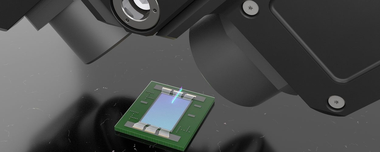
LMI offers the Gocator 5500 Series for such challenging applications. A Gocator 5512 sensor, as displayed in Figure 1, utilizes line confocal imaging technology for the accurate measurement and inspection of these challenging silicon wafers at each stage of the semiconductor manufacturing process.
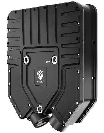
Figure 1. Gocator 5512 Smart 3D Line Confocal Sensor. Image Credit: LMI Technologies Inc.
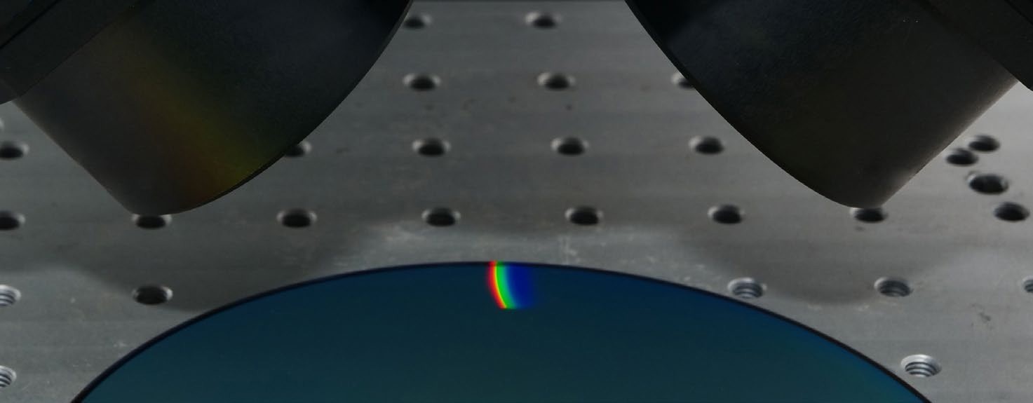
A Gocator 5500 Series sensor has a patented dual-axis design and can measure microscopic-scale dimensions and tomographic structures with high speed and accuracy. It projects a thin line of light onto a target surface and captures the reflected light with a line-shaped confocal aperture.
Any out-of-focus light is filtered out by the confocal aperture, with only the in-focus light being able to reach the sensor. By scanning the line of light across the target, the built-in software of the sensor can generate a 3D-point cloud of the scanned surface.
LCI technology provides several benefits compared to conventional optical measurement techniques, e.g., structure light or laser triangulation. For example, LMI’s smart 3D line confocal sensors have the ability to measure curved, translucent, transparent, and shiny objects and are unaffected by factory light conditions.
Additionally, Gocator 5500 sensors can inspect layers within transparent materials such as plastic or glass and deliver high-contrast intensity images that allow the detection of surface defects, including cracks, stains, scratches, and foreign materials within individual layers.
All the above is accompanied by sub-micron resolution and repeatability at high scan rates up to 16 kHz with PC acceleration.
The manufacture of semiconductors is extremely complex, with hundreds of steps that need precise control of pressure, temperature, light exposure, and chemical reactions. Any deviation from the optimal conditions may result in variations or defects that impact the reliability and functionality of the end product.
This is why semiconductor manufacturers must use advanced metrology and inspection tools to inspect every wafer at every stage of the process.
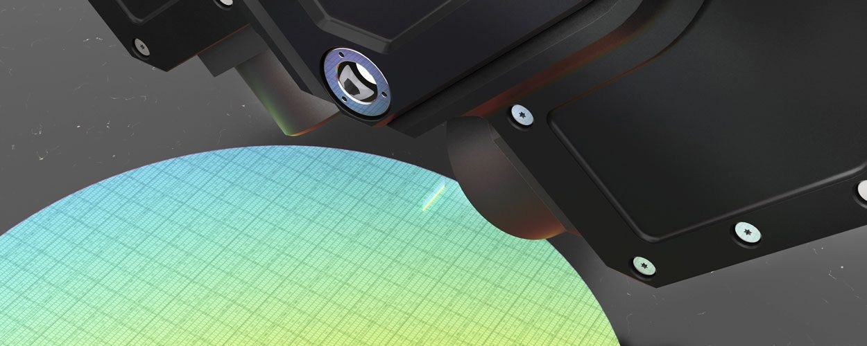
Gocator 5500 Series line confocal sensors are used for wafer sorting and dimensioning, in addition to many other essential applications in semiconductor manufacturing inspection. Image Credit: LMI Technologies Inc.
Semiconductor manufacturing quality control applications that can be solved with Gocator Smart 3D Line Confocal sensors include:
Wafer Inspection
Sorting
G5 sensors can measure the flatness, thickness, warp, bow, and notch alignment of silicon wafers with a sub-micron level of accuracy and repeatability. This allows the wafers to be quickly and efficiently sorted according to their specifications and quality.
Polishing Pad Inspection
G5 sensors can be used to scan the surface profile and texture of wafer polishing pads with nanometer resolution. This allows pad wear and condition to be monitored and for defects such as cracks, scratches, or foreign particles to be detected.
Dimensional Measurement and Defect Detection After Scribing
Following laser dicing and/or scribing, G5 Sensors can measure the accuracy of the groove depth and placement and the kerf width of the wafer scribing to prevent defects such as die chipping.
This enables more usable die per wafer and provides the maximum processing speeds and quality for the highest production throughput.
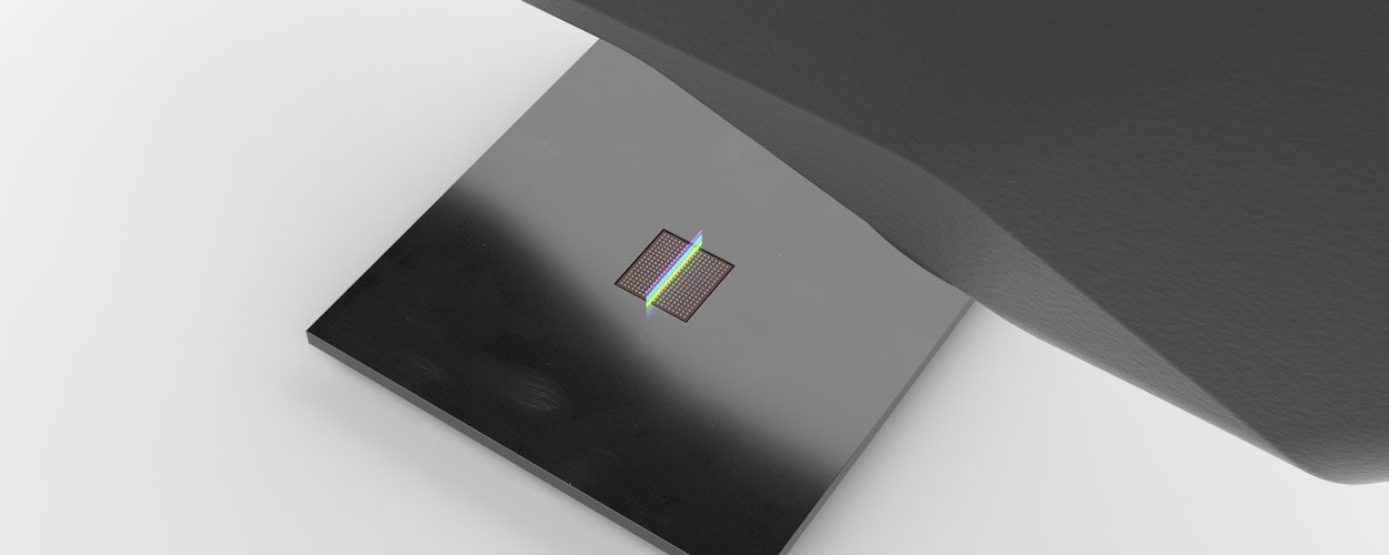
Semiconductor Wafer Inspection with Gocator 5500 Series Line Confocal Sensors. Image Credit: LMI Technologies Inc.
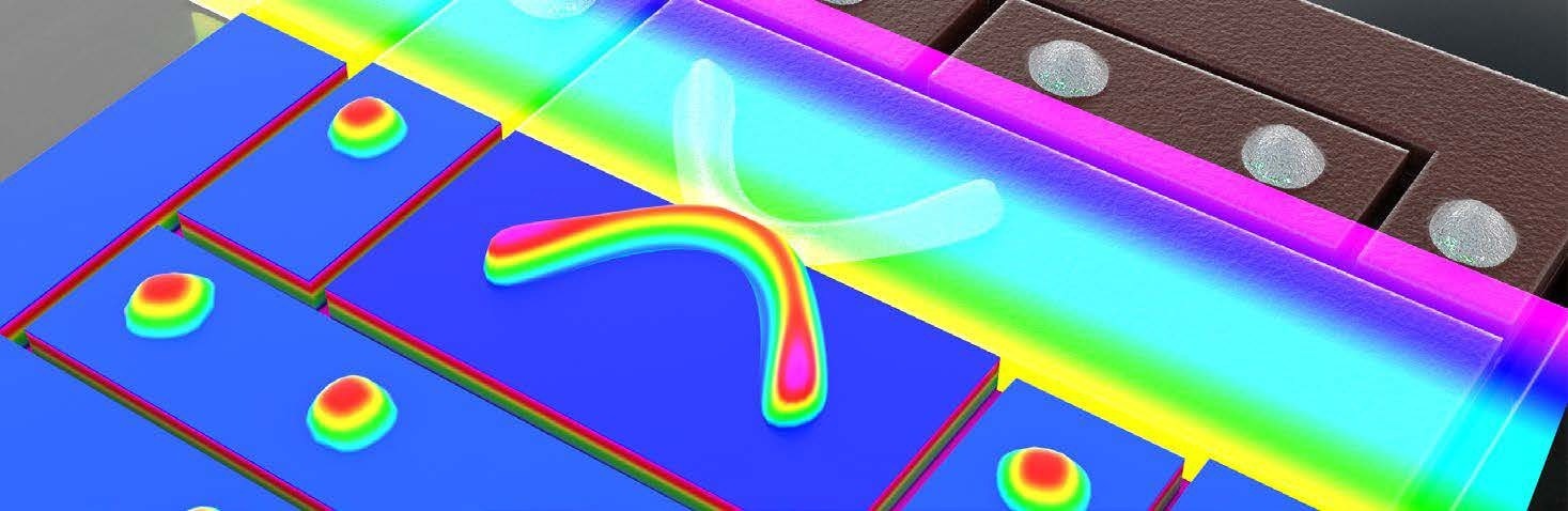
Inspection of BGA and PGA Position, Height, and Radius During Assembly and Test IC
Gocator 5500 sensors can be used to accurately measure ball position and height, as well as other dimensional information of the ball with a diameter of less than 50 microns.
The sensors can also inspect the position and height of the PGA pins to guarantee that there are no poor contacts produced during the subsequent insertion and removal process and to prevent defects from arising, such as pin damage from positional errors.
Additionally, the flatness and height of the joint position before welding are inspected to reduce the breakage of each solder joint after welding is completed.
Semiconductor BGA Inspection with Gocator 5500 Series Line Confocal Sensor. Image Credit: LMI Technologies Inc.
Inspection of Silver Epoxy During Die Application
Gocator 5500 sensors are used to accurately measure the surface area of coated silver epoxy in each lead frame area, in addition to the thickness or the height of the epoxy glue bead. For instance, the sensors can detect bubbles and measure the thickness of the glue bead.
Silver epoxy adhesive inspection with Gocator 5500 Series Line Confocal Sensor. Image Credit: LMI Technologies Inc.
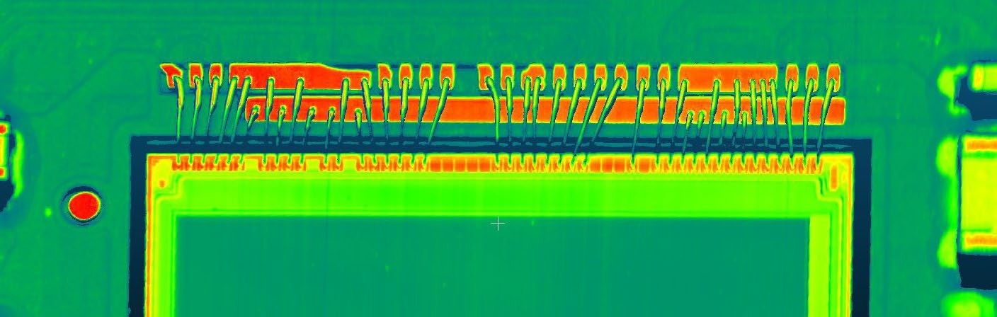
Defect Inspection During Wire Bonding Process
Gocator 5500 sensors measure the arch height and position of the wire with high accuracy, whether it is composed of copper, gold, or aluminum. These line confocal sensors can also detect defects such as bends or breaks in the wire.
Semiconductor Wire Bonding Defect Inspection with Gocator 5500 Series Line Confocal Sensor. Image Credit: LMI Technologies Inc.
Dimensional Measurement During Ball-Bumping Process
Gocator 5500 sensors can be used to accurately capture the height or thickness and diameter of the ball down to 2.5 microns. Additionally, the sensors can inspect the coplanarity between all ball bumps to detect any variation in height that can lead to uneven distribution of force, die fractures, and open circuits.
Semiconductor ball-bump diameter and height measurement with Gocator 5500 Series Line Confocal Sensor. Image Credit: LMI Technologies Inc.
Dimensional Measurement and Defect Inspection after Final Packaging
Gocator 5500 sensors capture the chip's width, length, and height after final packaging. The sensors can also generate high-resolution 2D grayscale images for the detection of defects such as scratches and pits.
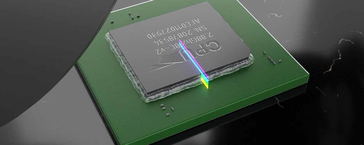
Final semiconductor packaging inspection with Gocator 5500 Series Line Confocal Sensor. Image Credit: LMI Technologies Inc.
Summary
In today’s semiconductor industry, there is a growing list of applications that LMI has solved using Gocator 5500 sensors.
Gocator 5500 sensors are the first sensors in the industry to combine LCI technology with a web-based interface, fast scan rates, onboard software, and multi-layer surface scanning ability.
These sensors also run GoPxL, LMI Technologies’ latest IIoT vision inspection software that comes with smart features such as built-in measurement tools, smart filters, and a custom HMI builder.

This information has been sourced, reviewed and adapted from materials provided by LMI Technologies Inc.
For more information on this source, please visit LMI Technologies Inc.