Feb 8 2016
Panasonic Corporation today announced that it has developed a new wide-dynamic-range[1] technology that can improve simultaneous-capture wide dynamic range[2] 100 times wider than conventional results can deliver, using a CMOS image sensor with an organic photoconductive film (OPF) *2.
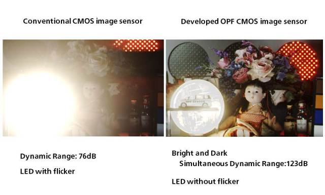 Difference of captured image between the conventional and the developed OPF CMOS image Sensor (Graphic: Business Wire)
With an OPF CMOS image sensor, the charge-storage function and photoelectric-conversion function can be set independently. By utilizing this unique feature of the OPF CMOS image sensor, overexposure can be prevented under bright conditions with no time distortion against moving objects. Moreover, a sharp and texture-rich image can be reproduced even under dark conditions. These technologies enable high-speed, high-precision imaging with no time distortion in high-contrast scenes. - more -
This newly developed wide-dynamic-range technology enables accurate imaging and reproduction of a richer color tone, even under high-contrast conditions (backlit scene or under studio lighting). In addition, synthesizing multiple exposure data captured at different times is unnecessary, thus enabling the accurate imaging of moving objects at high speed. The technology therefore enables high-speed, high-precision, and wide-dynamic-range imaging and sensing.
This new technology offers the following advantages.
- Wide incident angle (60 degrees), high sensitivity, high saturation and highly-functional circuits due to a unique feature of OPF that allows an OPF for photoelectric-conversion and readout circuits to be independent.
- 123dB simultaneous-capture wide dynamic range (100x wider than that of common silicon image sensors*3), while maintaining conventional chip size, due to our original “simultaneous-capture structure.”
This wide-dynamic-range technology includes the following.
- OPF CMOS Image Sensor Design Technology, where the photoelectric-conversion part and circuit part can be designed independently.
- Dual-Sensitivity Pixel Technology featuring two sensitivity detection cells (one for brightness; one for darkness) in each pixel, taking advantage of the high-saturation performance and flexibility of the OPF CMOS image sensor sensitivity setting in order to achieve a simultaneous-capture wide dynamic range.
- Capacitive-Coupled Noise Canceller Technology that can cancel pixel reset noise to improve S/N[3] characteristics when imaging dark objects.
Panasonic holds 58 Japanese patents and 44 overseas patents (including patents pending) related to this technology.
Panasonic presented some of these technologies at the international academic conference: ISSCC (International Solid-State Circuit Conference) 2016 that was held in San Francisco from January 31 - February 4, 2016.
Notes:
*1: As of February 2, 2016, based on data available to Panasonic.
*2: We employ an organic photoconductive film (OPF) developed by FUJIFILM Corporation.
*3: Comparison with Panasonic silicon CMOS image sensor.
Source: http://www.panasonic.com/