Metalenz, the first company to commercialize meta-optics, and STMicroelectronics (NYSE: STM), a global semiconductor leader serving customers across the spectrum of electronics applications, today announce that ST’s currently released VL53L8 direct Time-of-Flight (dToF) sensor is the highly anticipated market debut of the meta-optics devices developed through their partnership, which was disclosed in June 2021.
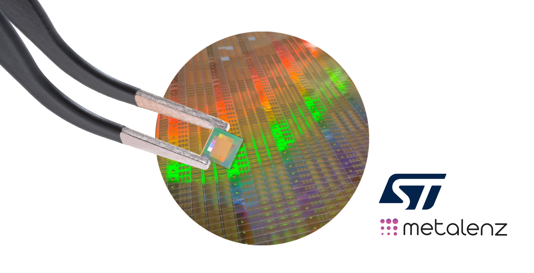
Image Credit: Metalenz
Metalenz’s Harvard-born, meta-optics technology can replace existing complex and multi-element lenses and provide additional functionality with a single meta-optic embedded in time-of-flight (ToF) modules from ST, the leading company in supplying 3D sensing modules. The introduction of Metalenz technology in these modules brings performance, power, size, and cost advantages to a multitude of consumer, automotive, and industrial applications. This marks the first time metasurface technology is commercially available and being used in consumer devices.
Unlike traditional molded and curved lenses, Metalenz’s novel optics are completely planar. Planar metasurface optics are now being manufactured on silicon wafers alongside electronics in ST’s semiconductor front-end fabs for the first time. The meta-optics collect more light, provide multiple functions in a single layer, and enable new forms of sensing in smartphones and other devices, while taking up less space. Metalenz’s flat-lens technology replaces certain existing optics in ST’s FlightSense™ ToF modules, which serve applications such as smartphones, drones, robots, and vehicles. In these, ST has sold more than 1.7 billion units to date.
“More than a decade of foundational research has brought us to this point. Market deployment of our meta-optics makes this the first metasurface technology to become commercially available. ST’s technology, manufacturing expertise, and global reach allow us to impact millions of consumers. We have multiple wins that mark the first application of our platform technology and we are now designing entire systems around its unique functionality. Our meta-optics enable exciting new markets and new sensing capabilities in mobile form factors and at a competitive price.”
Rob Devlin, co-founder and CEO of Metalenz
ST is a leader and leading innovator in ToF sensing technology that uses the speed of light to accurately calculate proximity. The sensor precisely measures the time a photon, traveling at 299,792,458 meters/sec, takes to travel to and reflect back from a surface. From its first ToF sensor, ST and its technology have helped revolutionize autofocus in smartphone cameras and, with presence detection and gesture recognition, improve security and power efficiency in mobile and computing applications.
Perfectly complementing ST’s advanced manufacturing capabilities and ToF technology, the introduction of products embedding Metalenz’s game-changing metasurface optics now enables significant power efficiency, optical performance, and module-size optimization that all bring benefit across consumer, industrial, and automotive markets,” said Eric Aussedat, Executive Vice President and General Manager of ST’s Imaging Sub-Group. “Initially targeting applications using near-infrared wavelengths, especially for 3D sensing, the products we’re introducing with Metalenz are perfectly suited for applications like face authentication, camera assist, consumer LIDAR, and AR/VR, where depth mapping is needed.”
The partnership of Metalenz IP with ST Manufacturing Technology brings the incredible accuracy and precision of electronics chip industry to make very precise and repeatable meta-optics that unlock this completely new way to make lenses that combine very high quality and large-scale cost-effective manufacturing.
About Metalenz
Metalenz, founded in 2016, is the first company to commercialize meta-optics. With exclusive worldwide license to the portfolio of foundational intellectual property relating to metasurfaces developed in the Capasso Lab at Harvard University, Metalenz has more than 20 patents on innovations that simplify and improve optical devices across multiple markets. The company’s meta-surface technology provides complex, multifunctional optical performance in a single semiconductor layer, relocating large-scale production of optics to semiconductor foundries—printing lenses like computer chips. Metalenz launched out of stealth in 2021 with funding from leading investors including 3M Ventures, Applied Ventures LLC, Intel Capital, M Ventures, TDK Ventures, and Foothill Ventures. Now in market, Metalenz optics will be in millions of consumer devices this year. To partner with Metalenz and learn more about how they’re revolutionizing optical sensing in consumer electronics and beyond, visit: metalenz.com.
About STMicroelectronics
At ST, we are 48,000 creators and makers of semiconductor technologies mastering the semiconductor supply chain with state-of-the-art manufacturing facilities. An integrated device manufacturer, we work with more than 200,000 customers and thousands of partners to design and build products, solutions, and ecosystems that address their challenges and opportunities, and the need to support a more sustainable world. Our technologies enable smarter mobility, more efficient power and energy management, and the wide-scale deployment of the Internet of Things and connectivity. ST is committed to becoming carbon neutral by 2027. Further information can be found at www.st.com.