Jun 18 2010
The Department of Energy’s (DOE) program, related to the Small Business Innovation Research (SBIR), has provided a grant to Arradiance for developing large-area microchannel plates that will be utilized as a substitute for conventional photomultipliers.
This grant has been provided to develop an inexpensive plate up to a maximum 8” x 8” size. The plate will be utilized in MCP-based photomultipliers (MCP-PMTs). These plates will be tiled together in a manner to achieve fast and large detectors that will be used in projects, such as the large neutrino detectors being developed by the National Science Foundation presently.
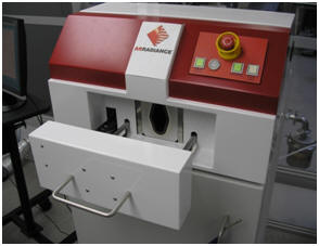 Arradiance GEM-D2 ALD System
Microchannel plates are being utilized for many detection and imaging applications where high temporal and spatial resolution along with high signal to noise ratio features are vital. Examples of its applications include night vision, biotechnology, homeland security, earth-observing and astrophysical and satellite instrumentation, and analytical instrumentation.
It is possible to construct these plates in larger sizes without resorting to the use of the expensive lead-glass multiple draw technique. This ability will help in market penetration of these plates through improved overall performance and reduced cost for any detector in which these plates are used as components.
Arradiance’s CTO Neal Sullivan, informed that the increment in performance of the microchannel plate was just marginal for decades due to adoption of a production process that was restricted by existing materials and sub processes. He explained that the necessary lead glass substrate material resulted in restricting the capability for optimizing the performance of the microchannel plate for applications where the substrate size, lifetime, gain, and composition are important.
He explained that the proprietary nanofilm technology of Arradiance has enabled fabrication of microchannel plates using various substrate materials. These materials include non-lead or lead containing glasses, plastic, ceramics and silicon. He added that the nanofilms are independent of the substrate material, resulting in optimized performance and adoption of larger substrate sizes.
Source: http://www.arradiance.com.