Sony Corporation (“Sony”) today announced that it will establish Sony Semiconductor Corporation (“SCK”) Yamagata Technology Center (“Yamagata TEC”) on March 31, 2014, utilizing the Tsuruoka Factory semiconductor-related assets held by Renesas Yamagata Semiconductor Co., Ltd. (“Renesas Yamagata Semiconductor”), which are scheduled to be transferred to Sony in accordance with the definitive agreement that Sony and Renesas Electronics Corporation (“Renesas Electronics”) executed and jointly announced on January 29, 2014.
SCK Yamagata TEC will serve as a new production site for CMOS image sensors, and Sony plans to engage in capital investment from the first half of the fiscal year ending March 31, 2015 (“FY14”) through the second half of the fiscal year ending March 31, 2016 (“FY15”) in order to increase image sensor production capacity.*1 This planned investment forms part of Sony’s mid- to long-term plan to increase its total production capacity for image sensors from the current capacity of approximately 60,000 wafers per month to approximately 75,000 wafers per month.*2 Following the acquisition, Sony intends to convert part of the semiconductor manufacturing equipment that Sony is scheduled to acquire from Renesas Yamagata Semiconductor to CMOS image sensor manufacturing equipment, and also to install new manufacturing equipment for CMOS image sensors in Yamagata TEC. Yamagata TEC will primarily engage in the manufacture of photodiodes and wiring processes for stacked CMOS image sensors.*3
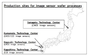
Stacked CMOS image sensors enable superior image quality and advanced functionality with compact size. Demand for these image sensors is anticipated to further increase, particularly within the expanding market for mobile devices such as smartphones and tablets. Sony will position Yamagata TEC as a new site for one phase of the image sensor wafer production process, alongside its existing Kagoshima Technology Center, Kumamoto Technology Center, and Nagasaki Technology Center sites. By doing so, Sony aims to strengthen its capacity to supply stacked CMOS image sensors and further reinforce its leading position in the image sensor industry. Sony is also continuing to accelerate the revitalization of its electronics business by incorporating its image sensors, such as these advanced stacked CMOS image sensors, into a wide range of products across its core imaging and mobile businesses.
The total investment amount is expected to be approximately 35 billion yen, comprising (i) approximately 7.5 billion yen to acquire Renesas Yamagata Semiconductor’s Tsuruoka Factory assets in the fiscal year ending March 31, 2014 (“FY13”), and (ii) approximately 27.5 billion yen for planned capital investment to be carried out during FY14-FY15.
Sony is currently evaluating its consolidated financial results forecast for FY13 to take into account the FY13 portion of the investment and other factors. For details, please refer to “Renesas Electronics and Sony Sign Definitive Agreement to Transfer Semiconductor Manufacturing Facility and Equipment, etc.” which was jointly announced on January 29, 2014.
http://www.sony.net/SonyInfo/News/Press/201401/14-0129E/
*1: The establishment of Yamagata TEC and the related investment are subject to the completion of the Tsuruoka Factory’s asset acquisition by SCK.
*2: The total production capacity (300mm wafer basis) includes the output of foundry operations to which Sony outsources a part of the manufacturing process. For the purposes of calculating total production capacity, the capacity of the 200mm wafer production lines in Kagoshima Technology Center and Nagasaki Technology Center has been converted to the new 300mm wafer production capacity basis.
*3: “Stacked CMOS image sensors” are CMOS image sensors in a stacked structure that layer the pixel section containing back-illuminated structure pixels onto chips containing the circuit for signal processing, as an alternative to the supporting substrates used in conventional back-illuminated CMOS image sensors.
Source: http://www.sony.net/