Platypus Technologies has introduced patterned gold thin films on glass, produced through e-beam metal evaporation.
The titanium adhesion layer between glass and gold enhances the mechanical stability of the gold film. Gold films have a high purity of 99.999% and exhibit low surface roughness (nanometer-scale roughness).
Such electrodes are produced without using organic or photoresist organic solvents that may otherwise contaminate the gold surface. They are perfect for use in MEMS biosensors (bioMEMS), microelectrodes and chemical sensor chips.
Features
- Low surface roughness for high resolution and sensitivity
- Exceptional reproducibility
- Transparent glass substrate allows optical analysis
- High purity gold; does not require pre-cleaning
Resistivity Electrode
Resistivity electrode is a five-probe microelectrode that can be used for quantifying sheet resistance (for example, Kelvin method or four-point probe), conductivity or impedance of biological tissues, advanced materials, 2D materials, polymers and nanomaterials. Finger width is 160 ± 10 µm; gap distance is 345 ± 5 µm; and chip dimensions are 20 x 10 x 0.7 mm. Each pack includes eight chips.
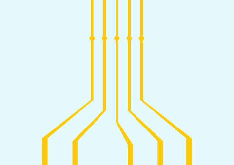
Image Credit: Platypus Technologies LLC
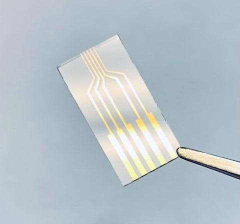
Image Credit: Platypus Technologies LLC
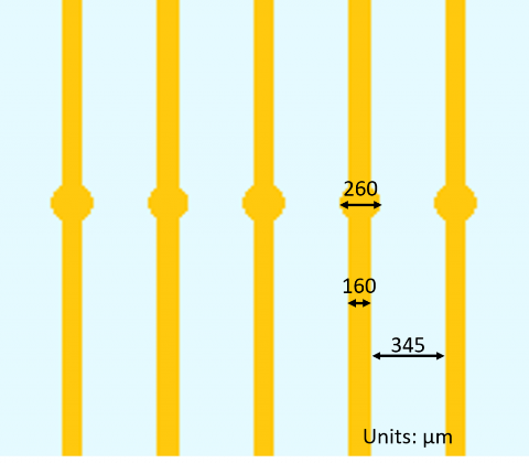
Image Credit: Platypus Technologies LLC
Three-Probe Electrode
The three-probe microelectrode chip is perfect for developing and testing novel chemical sensors. Metal patterned electrodes provide excellent conductivity and enable optical imaging of the sensing layer.
Applications comprise transistors (HEMTs, FETs and BioFETs), biosensors and chemical sensors. Finger width is 150 ± 5 µm; gap distance is 350 ± 5 µm; and chip dimensions are 20 x 10 x 0.7 mm. Each pack includes eight chips.

Image Credit: Platypus Technologies LLC
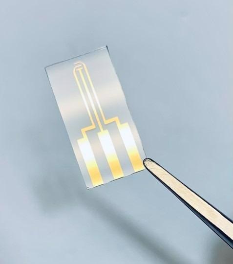
Image Credit: Platypus Technologies LLC
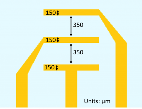
Image Credit: Platypus Technologies LLC
Disk Electrode
The disk electrode chip is perfect for performing electrochemical experiments of droplets and solutions through cyclic voltammetry or electrochemical impedance spectroscopy (EIS). The center disk electrode acts as a working electrode, whereas either one of the side electrodes can act as a reference electrode or auxiliary electrode.
Finger width is 270 ± 5 µm; gap distance is 490 ± 7 µm; chip dimensions are 20 x 10 x 0.7 mm, and the diameter of the working electrode is 590 ± 5 µm. Each pack includes eight chips.

Image Credit: Platypus Technologies LLC
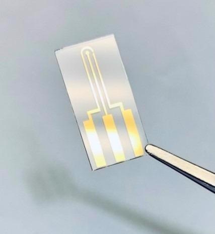
Image Credit: Platypus Technologies LLC
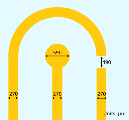
Image Credit: Platypus Technologies LLC
Custom Electrodes
If customers are unable to find their requirements, they can contact Platypus Technologies for their custom patterned microelectrodes. The company has the capabilities to coat a majority of metals, such as Ag, Au, Ti, Ni, W, Al, etc. on a number of substrates, with numerous design options. Platypus Technologies can even cut glass to any size (more than 5 mm).