Feb 4 2016
Panasonic Corporation today announced that it developed the CMOS image sensor (APD-CMOS) that uses avalanche photodiodes (APDs)*1 in each pixel. The company has succeeded in obtaining 10,000 times multiplied*2 electric signals by means of the APDs' multiplication of photoelectrons that are generated by photoelectric conversion in the photodetector. This allows you to take sharp color images even under starlight (illuminance of 0.01 lux) or in other similarly dark places.
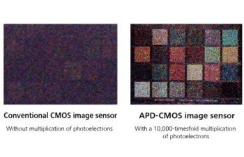 Comparison of images without multiplication and with multiplication under 0.01 lux illuminance (Graphic: Business Wire)
*1 Photodiodes that are capable of obtaining large electric signals from weak light (i.e. small numbers of photons). Large output signals can be obtained by multiplying photoelectrons that are generated in the photoelectric conversion layer.
*2 In comparison with image sensors without a multiplication function (according to our own research as of February 3, 2016)
This new image sensor allows for highly sensitive imaging through the multiplication of photoelectrons, realizing high-gradation color imaging without the need to increase the exposure time even in dark places. In addition, the multiplication of photoelectrons can be controlled instantly by changing the voltage applied to the APDs depending on the illuminance at the time of imaging, allowing you to take images at various illuminances from bright places to dark places. Its expected applications include surveillance cameras that require color imaging with a wide dynamic range and industrial cameras that require ultra-highly sensitive imaging.
This development brings the following advantages.
- Highly sensitive color imaging:
40 million/lux・sec・μm2 (10,000 times sensitive in comparison to conventional devices)
- Wide dynamic range:
100 dB (+ 40 dB in comparison to conventional CMOS image sensors)
This development has been realized on the basis of the following technologies:
- APD picture element design technology in which avalanche photodiodes and charge storages are incorporated in the photoelectric convertor for not only multiplying but also accumulating photoelectrons that contain generated color information
- Variable sensitivity technology in which multiplication is controlled in a thousandth of a second by controlling the voltage applied to the APDs, realizing 30-fps video imaging that can follow the changes in illuminance
With conventional image sensors, photoelectrons that are photoelectric-converted during imaging in dark places may fall below the noise level, thereby limiting the imaging environment to no less than moonlight (illuminance of 0.1 lux) or so. This is why imaging under illumination of a near-infrared light source and imaging using photo multipliers have been carried out. However, near-infrared light sources have the drawback of the inability of color imaging, whereas photo multipliers have the drawback of forcing cameras to be upsized due to the necessity of a large-capacity power supply.
This development result was announced in the 2016 International Solid-State Circuits Conference, which was held in San Francisco on February 1, 2016.
Source: http://panasonic.net/