X-ray photoelectron spectroscopy (XPS) is a unique technological innovation that produces empirically tested, quantitative information on the composition of compound semiconductor alloys. Using Kratos AXIS Nova spectrometer, a study was done to analyze novel SPLED structures are to characterize AI content. The depth profile of the full device was acquired through conventional profiling methods with Shard stepwise rotation. Through the AI content, it was confirmed that various expected compositions were present in different layers. This finding could be used in creating a model for the performance of cell structures.
Compound semiconductors are used in electronic applications with specialist requirements. Because of this, the material is considered a primary sustainable technology in optoelectronics. The successful use of compound semiconductors may be associated with the ability to electronically and optically alter the properties of the alloy; in particular, its alloy composition (binary, ternary, quaternary, or quinary) and heterostructures.
A report by Allied Market Research showed that the global compound semiconductor market was valued at $66 billion in 2016 and is expected to increase its worth to $143 billion by 2023. This projection clearly shows the important role of composition in compound semiconductors; however, its accurate determination, especially among devices with many different layers, remain a challenge. A pertinent example of this issue are devices that contain Distributed Bragg Reflectors (DBRs)—alternating layers of high- and low-refractive index materials that create a stop-band in which a set of wavelengths are almost fully reflected. For example, Vertical Cavity Surface Emitting Lasers (VCSELs) are relatively inexpensive semiconductor lasers that utilize DBEs to form mirrors of the lasing cavity.
Retaining the quality and consistency of DBRs is important because VCSELs have average gain lengths that are 105 times smaller than those of edge-emitting lasers. This implies that VCSELs need ultra-high reflectivity mirrors to achieve a reasonable threshold current. Other devices that use DBRs are Single-Photon LEDs (SPLEDs) that are utilized in quantum key distribution in quantum cryptography networks.
 Please click here if you would like more information on the instrument used in this article or a quote
The demand for VCSELs in the field of communications continues to rise, even while non-communication markets are expected to grow eight-fold by 2022.
A study focusing on DBRs was done in order to accurately characterize its structure, including the determination of an anticipated precedence of semiconductor layer growth. To further characterize the growth, X-ray photoelectron spectroscopy (XPS) depth profiles were utilized to measure the chemical composition of DBR layers. It is expected that minute changes in AI composition would immediately affect the refractive index, ultimately changing the optical path length of the layer. Consequences in mirror characteristics to laser output wavelength are expected to be observed. Device performance is also directly related to XPS quantitative information on AI content for the DBR structure.
Experiment
An XPS analysis was done using the Kratos AXIS Nova spectrometer on a SPLED structure that was grown through molecular beam epitaxy at Lancaster University in the United Kingdom. A Minibeam IV focused ion gun was used for depth profiling in 4 keV Ar+ mode. In order to remove energetic neutrals and prevent the degradation of the interface resolution, the ion source was made to have a bend in the ion column.
Furthermore, a sample rotation using 90o increments at each etch cycle was utilized in order to minimize the roughening of samples during etching. At the same time, compucentric rotation may also be implemented using a simple tick-box in the ESCApe acquisition software.
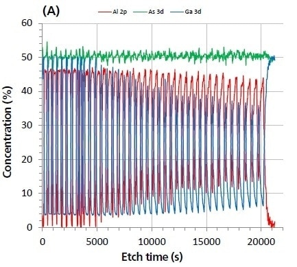
Figure 1A. Complete depth profile of SPLED structure.
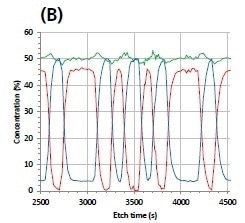
Figure 1B. Zoomed-in emitter region.
Results
The SPLED wafer was mounted onto the rotation platen before being loaded onto the instrument. Meanwhile, depth profiling was performed using high-energy monoatomic 4 keV Ar+ ions with the focused beam centered on the surface to create a uniform etch crater. XP spectra were acquired after each etch cycle in order to determine the composition of the newly-exposed surface. Small-spot spectroscopy was also utilized to limit the influence of crater edge effects on the interface resolution.
These set-ups resulted in a dramatic variation in AI content found within alternating GaAs/Alx Ga1-x As layers. In this particular structure, the Alx Ga1-x As layers were designed to have an AI fractional content (x) of 0.9 and an elemental content of 45%. Quantitative data from the XPS also showed a consistent value of ~46% for the Alx Ga1-x As layers which fall within the acceptable limits of expected experimental results.
Apart from these findings, it was found that the composition of the emitter layer is also consistent with the desired composition; however, after etching through the material for several further mirror layers, the profile began to lose form. This may be due to the blending and roughening of layers from the ion etching process, a known issue in such mode.
Due to the total thickness of the layers that would greatly impact total experiment time, it also became unfeasible to repeat the experiment using low-energy ion (250 – 500 eV). As an alternative, post-acquisition XP images were acquired for Al 2p and Ga 3d photoelectron lines to determine etch crater shape and positioning. The images clearly showed the layer structure and the presence of an emitter layer that is eight repeat units into the device.
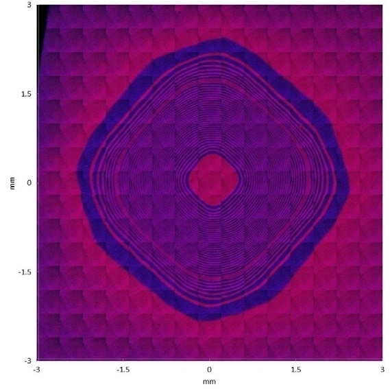
Figure 2. Stitched XPS image of etch crater; Ga (RED) Al (BLUE).
Acknowledgements
Many thanks go to Tom Wilson, Peter Hodgson, Alex Robson and Manus Hayne for sample preparation and fruitful discussions, who would like to acknowledge EPSRC (grant number EP/P034233/1) and to IQE plc for financial support, through a CASE Award for Tom Wilson.
References and Further Reading
- alliedmarketresearch.com/compound-smiconductor-market, accessed 2/2/2018.
- yole.fr/IR_LED_LASER_MARKET_TRENDS.aspx#.WnSRQklLFaQ, accessed 2/2/2018.
- P. Moser, “Energy efficient oxide confined VCSELs for optical interconnects in data centers and supercomputers”, PhD thesis, Technische Universitt Berlin, Fakultt II - Mathematik und Naturwissenschaften (2015).
- paneuropeannetworks.com/science-technology/quantum-rings-torule-them-all/, accessed 2/2/2018.
- lancaster.ac.uk/physics/research/experimental-condensed-matter/ quantum-nanotechnology/, accessed 2/2/2018.

This information has been sourced, reviewed and adapted from materials provided by Kratos Analytical, Ltd.
For more information on this source, please visit Kratos Analytical, Ltd.