Polytec Micro System Analyzers are one of the most commonly used evaluation tools within MEMS laboratories. This is most likely also the case in many laboratories across the world. Here are three examples where Polytec tools have been used in MEMS studies.
High Frequency Disk-Type MEMS Resonators
Gyroscopes, mass sensors, optical scanners, clock oscillators etc. all use mechanical resonance. It is one of the key dynamics exhibited by MEMS. The pursuit of higher resonance frequencies and new applications for these is an obvious research topic for MEMS. The two main areas of interest are electrostatic and piezoelectric. As such, electrostatic MEMS resonators were studied in greater detail from early on. However, electromechanical coupling is too weak for many applications – a critical problem for electrostatic transduction. For this reason, piezoelectric transduction was adopted for disk-type resonators. In several previous studies these were based on electrostatic transduction
Piezoelectric disk-type resonators mechanically connected via a center silicon disk are shown in Figure 1 [1]. A piezoelectric thin film was made up of sputter-deposited aluminum nitride (AlN). The frequency characteristics up to 400 MHz are shown in Figure 2, where specific resonance modes are represented as individual peaks. The main mode required was the (2,4) mode at 292.8 MHz. Figure 3 shows the finite element method (FEM) which can be used to calculate the mode shapes. The small size and high frequency make it difficult to determine the actual mode shape. Polytec’s UHF-120 was used in this study to determine the actual mode shape of the disk-type resonators [2].
Polytec’s UHF-120 is a high-frequency laser Doppler vibrometer, with the ability to measure velocity and integrated displacement up to 1,200 MHz. The displacement amplitude resolution is 2 pm @4.88 kHz resolution bandwidth. Measured (2, 3) and (2, 4) mode shapes are given in Figure 4. The calculated and actual mode shapes shown in Figures 3 and 4 respectively look somewhat dissimilar. This is precisely why it is necessary to experimentally characterize and validate modeled data. Furthermore, misalignment of lithographic patterning may have caused the locally large amplitude found at the left upper part. As a result, it was concluded that piezoelectric disk-type MEMS resonators are unsuitable for commercial frequency control applications. Polytec’s UHF-120 was, however, demonstrated to be useful for observing high frequency MEMS resonators.
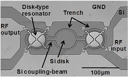
Figure 1: Mechanically-coupled piezoelectric disk-type MEMS resonators.
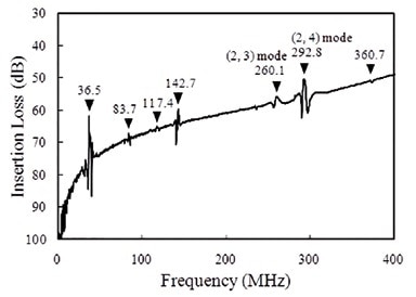
Figure 2: Frequency characteristics of disk-type MEMS resonators shown in Figure 1.
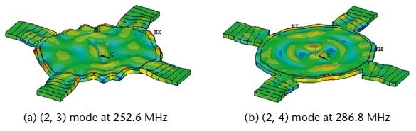
Figure 3: Mode shapes calculated by FEM.
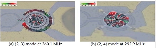
Figure 4: Mode shapes observed by scanning laser vibrometry using Polytec UHF-120.
Laterally-Driven PZT Actuator
In MEMS design, an actuator is often a limiting factor. A small actuator with strong forces and large displacements is what everyone strives for. However, this is too much to expect from a MEMS device. It is also expected that new MEMS actuators have better performance alongside new functions that further extend MEMS applications.
A recently developed PZT MEMS actuator is shown in Figure 5 [3]. The actuation is based on the bending motion of a PZT thin film. This means that PZT MEMS actuators will normally move in an out-of-plane vertical direction. However, our new actuator moves in an in-plane lateral direction.
The mechanism of the laterally driven PZT actuator is demonstrated in Figure 6. Silicon trenches 2 µm deep are filled with sol-gel-based nano-composite PZT to form a cantilever made up of a laterally stacked PZT/silicon/ PZT structure. Atomic layer deposition (ALD) was used on both sidewalls of each PZT to form thin platinum layers as driving electrodes. The new actuator is much smaller than conventional comb-type electrostatic actuators as the cantilever itself bends with a bimorph mechanism. A standard MEMS evaluation tool, Polytec’s MSA-500, was used to characterize the fabricated actuator (Figure 5). This serves as a scanning laser Doppler vibrometer, a white light interferometer and a stroboscopic video microscope.
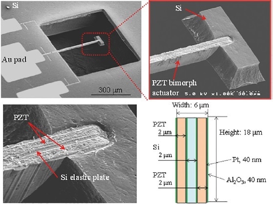
Figure 5: Laterally-driven PZT actuator with high aspect ratio PZT/Si/PZT structure.
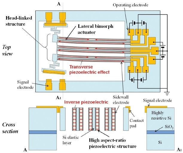
Figure 6: Mechanism of laterally-driven PZT actuator.
1PZT: Lead zirconate titanate (PZT) is an intermetallic inorganic compound that consits of lead (Pb), oxygen (O) and tita- nium(Ti) or zirconium (Zr). It is a ceramic perovskite material that shows a marked piezoelectric effect.
The low temperature co-fired ceramic (LTCC) wafer has been jointly developed by Nikko Company (Ishikawa, Japan) and MEMS and can be anodically bonded with a silicon wafer [4]. The LTCC material contains sodium ions which provide ion conductivity above 300°C and thus has a coefficient of thermal expansion similar to that of silicon. The anodic bonding characteristic is identical to that of borosilicate glass. Produced by stacking and firing punched green sheets, the anodically-bondable LTCC wafer provides screen-printed metal interal wiring (Figure 8).
Lateral motion of MEMS actuators can be observed using a stroboscopic video microscope. A decay vibration of the cantilever measured by the MSA-500 is shown in Figure 7. The data in Figure 7 were Fourier transformed, to give 14.26 kHz as the fundamental resonance frequency (f0). Furthermore, after the selective wet etching of the PZT, the density of the PZT (ρPZT) was measured from the difference in weight. Then, Young’s modulus of the PZT was calculated from f0 and ρPZT. At a driving voltage of 25/0 V (unimorph actuation) and 25/−5 V (bimorph actuation) the static tip deflection of the cantilever was 5 µm and 10 µm, respectively. Finally, we estimated the d31 piezoelectric constant to be 36 pC/N.
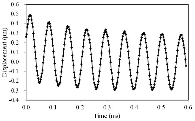
Figure 7: Decay vibration of laterally-driven PZT actuator measured by stroboscopic video microscopy using Polytec MSA-500.
Figure 8: Cross section of anodically-bondable LTCC wafer.
Wafer-Level Hermetic Packaging with Anodically-Bond- Able LTCC Substrate
Tiny moving and/or suspended structures, sealed hermetically to protect from moisture, dust and other contamination, air damping control, thermal isolation etc. are included with MEMS. The size and cost of MEMS is greatly impacted by packaging. As such, wafer-level packaging is key for their business. Wafer-level hermetic packaging is currently created through the anodic bonding of a borosilicate glass lid wafer with a silicon MEMS wafer. While anodic bonding is simplistic, reliable and of high yield, a critical problem is how to electrically access MEMS hermetically sealed in a cavity.
Porous gold bumps in parallel with anodic bonding can be used to electrically connect the metal vias in the LTCC wafer and MEMS on a silicon wafer. Further details can be found in [5, 6]. Silicon diaphragms were used to assess the reliability of hermetic sealing. The LTCC wafer and a silicon wafer with diaphragms were anodically bonded in vacuum. Following on from this, Polytec’s MSA-500 white light interferometry was used to measure the deformation of the diaphragms in air. There was negligible deformation of the diaphragms during a thermal cycling test (40°C × 30 min/125°C × 30 min) (Figure 9).
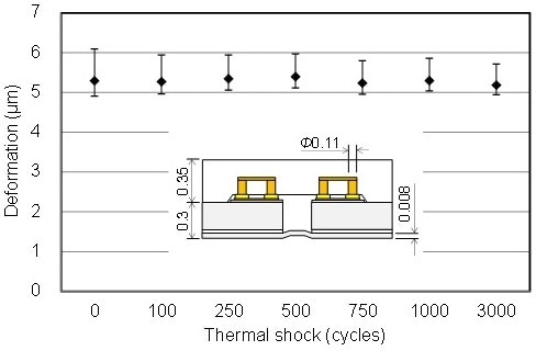
Figure 9: Reliability of hermetic packaging using anodically-bondable LTCC wafer.
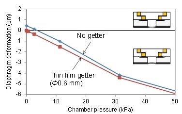
Figure 10: Sealing pressure measurement by zero balance method (Degassing at 400 °C for 30 min → Anodic bonding at 400 °C and 600 V for 1 min, Cavity volume = 0.26 mm3)
Through the resistance of daisy-chain connections, high reliability of electrical interconnection through the porous gold bumps was also demonstrated.
Aside from reliability, another concern is pressure in a vacuum-sealed cavity. Pressure in the sealed cavity is often higher than that of bonding environment as anodic bonding generates oxygen gas.
The diaphragm with the zero-balance method in a vacuum chamber was used to measure the pressure in the sealed cavity. The chamber pressure when the diaphragm was flat is known as the sealing pressure. To compensate the influence of a vacuum window the special optics was attached to the objective lens of the MSA-500. Examples of measured data are shown in Figure 10. The sealing pressure was lower than the detecting limit (approximately 80 Pa in this experiment) when a thin film non-evaporable getter (NEG) was used.
References
- Takeshi Matsumura et al., Multi-band radio-frequency filters fabricated by using polyimide-based membrane transfer bonding technology, Journal of Microme- chanics and Microengineering, 20 (2010) 095027
- Takeshi Matsumura et al., Vibration Mode Observation of Piezoelectric Disk-Type Resonator by High-Fre- quency Laser Doppler Vibrometer, Electronics and Communications in Japan, 95 (2012) pp. 33–41
- Shinya Yoshida et al., Fabrication and character- ization of laterally-driven piezoelectric bimorph MEMS actuator with sol–gel-based high-aspect- ratio PZT structure, Journal of Micromechanics and Microengineering, 23 (2013) 065014
- Shuji Tanaka et al., Wafer-Level Hermetic Packaging Technology for MEMS using Anodically-Bondable LTCC Wafer, 24th IEEE International Conference on Micro Electro Mechanical Systems, Cancun, Mexico, January 23–27, 2011 pp. 376–379
- Shuji Tanaka et al., Versatile Wafer-Level Hermetic Packaging Technology using Anodically-Bond- able LTCC Wafer with Compliant Porous Gold Bumps Spontaneously Formed in Wet-Etched Cavities, 25th IEEE International Conference on Micro Electro Mechanical Systems, Paris, France, January 29–February 2, 2012, pp. 369–372
- Shuji Tanaka et al., Electrical Interconnection in Anodic Bonding of Silicon Wafer to LTCC Wafer Using Highly Compliant Porous Bumps Made from Submicron Gold Particles, Sensors and Actuators A, 188 (2012) pp. 198–202

This information has been sourced, reviewed and adapted from materials provided by Polytec.
For more information on this source, please visit Polytec.