In the flat-panel display market, OLEDs (Organic Light-Emitting Diodes) are being launched as the next wave of technology.
This is attractive due to the fact that OLED displays guarantee enhanced display appearance for both large-format TVs and smartphones at a fraction of the cost and power of alternative display technologies.
OLEDs have optimized contrast ratios and detailed images with more vibrant colors and deeper blacks. They do not require backlight which creates a thin and lightweight display that consumes less electricity.
OLEDs also offer a significant increase in responsiveness, around 1,000 times faster than current technologies, essentially eliminating blur in 3D and fast-moving video.
As OLED manufacturers aim to offer OLED-based products that are commercially viable, the expensive costs involved with material prices and manufacturing yield problems have restricted OLED technology being adopted across the market, most significantly in large-format implementations, as they increase prices to the end-customer.
To date, the smartphone market has been the most effective segment for OLED technology and is prone to be the catalyst that boosts the adoption of OLEDs in alternative applications over the long term.
Display Supply Chain Consultants (DSCC) refers to smartphones as the leading OLED market, responsible for an estimated 91% of units each year with its revenue share projected at around 79% by 2022.1 This growth means that manufacturing efficiency will need improvements.
OLEDs have enhanced contrast ratios and more precise images with more vibrant colors and deeper blacks. They do not require backlight which results in a lightweight and thin display that consumes less electricity.
![Smartphone market leads the way for OLED adoption. [Source: DSCC’s Quarterly OLED Shipment and Fab Utilization Report]1](https://www.azosensors.com/images/Article_Images/ImageForArticle_1816_46137198326257812.jpg)
Figure 1. Smartphone market leads the way for OLED adoption. [Source: DSCC’s Quarterly OLED Shipment and Fab Utilization Report]1
The short-term market size is small for large-format OLED TVs, but analysts at DSCC estimate that TVs Will take second seat to smartphones, increasing to 42% market share by 2022, and succeeding LCDs by 2021.1
Manufacturers have found it challenging to attain consistent picture quality on large-format OLED displays creating low production yields.
This has an effect on the timing of viable market entry and maximizes retail prices for OLED large-screen TVs.
Present-day large screen OLED TVs are sold at prices into the thousands of dollars (USD), making inexpensive and high-definition LED and LCD choices more attractive to the wallets of consumers who care about their budget; the price point once the market adopts OLED in volume and replaces current technologies will be considerably lower.
OLED Manufacturing Challenges
OLED technology adds multiple special challenges to the system of manufacturing, despite the display size.
Line Mura
Material is deposited on a substrate to create the individual sub-pixels in the OLED process of manufacturing. If this process is not entirely the same, the end result may be line mura, which presents as clearly-defined vertical and/or horizontal orientation in the OLED display.
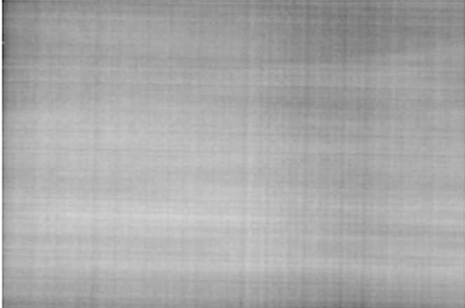
Figure 2. OLED display with uncorrected line mura.
Material is deposited on a substrate to create the individual sub-pixels in the OLED manufacturing process. If this process is not entirely the same, the end result may be line mura which will have clearly-defined vertical and/or horizontal orientation in the OLED display.
Sub-Pixel Luminance Performance
OLEDs utilize organic semiconductor material that is emissive. This means that it lights up after the application of the electric current. Due to this, OLED and different emissive displays (such as the emerging microLED and LED) do not need a backlight.
OLED display pixels are comprised of red, green, and blue sub-pixels. The output of every sub-pixel is controlled individually. Color and brightness (luminance) are established at the pixel level through the combination of the subpixel outputs.
There may be differences in luminance for the same electrical signal input across the population of uniformly-colored sub-pixels on the display due to discrepancies in production. This creates variations in brightness from pixel to pixel.
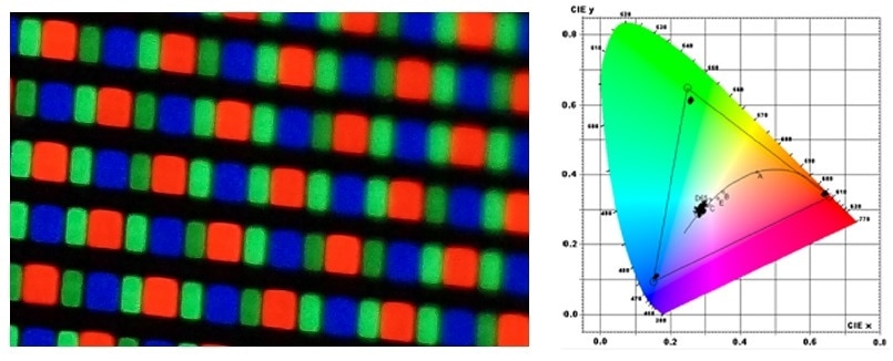
Figure 3. Sub-pixels combine to create pixels with various colors and brightness.
This sub-pixel-level variability in OLED and different emissive displays creates alternative issues with performance to what is found in LCDs.
In LCD panels, adjacent pixels tend to have equal luminance as LCDs utilize a shared backlight, so the brightness of adjacent pixels will be mostly the same.
To attain uniform and precise colors, the brightness of each distinct OLED subpixel must be strictly controlled.
Display Color Non-Uniformity
Decreased color accuracy and color non-uniformity throughout the display is another result of inconsistent brightness levels in the OLED display sub-pixels.
To attain uniform and precise colors, the brightness of each distinct subpixel must be strictly controlled.
In reality, even within a manufacturing system that has been well controlled, sub-pixels in OLED and alternative emissive displays will have extensive differences in brightness levels.
When these differences are not accounted for, there may be color non-uniformity throughout the display, decreasing the picture quality to possibly inadequate levels and decreasing production yields.
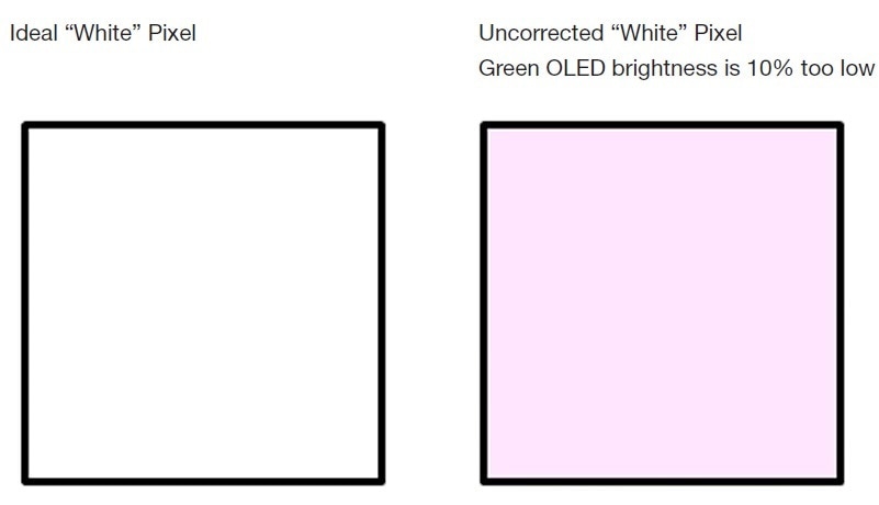
Figure 4. Incorrect brightness levels create non-uniformity in color across an OLED display.
Imaging Colorimeter Applications to OLED and Other Emissive Display Manufacturing
Imaging colorimetry-based display test systems have proved to be successful in enhancing quality and decreasing costs of production for both LED and LCD display screens.
Testing applications cover tablets, smartphones, monitors, laptops, digital billboards, and TVs.
These verified methods can be adapted to OLED and different emissive display production testing along with allowing manufacturers to use this technology in the same devices with the same beneficial return on investment.
The two main elements of a display test system are:
1. Imaging Colorimeters which enable the precise measurement of display visual performance that is equal to human perception of color, brightness, and spatial (or angular) relationships.
High-performance imaging colorimeters can effectively analyze the luminance (brightness) of distinct sub-pixels in an emissive display such as OLED along with the overall uniformity of the display.
2. Test Execution and Analysis Software which is production-line software for image analysis to locate quality issues and defects, evaluate their magnitude, and compute the measurements in order to make pass or fail determinations.
This software can also comprise of display performance correction techniques that can be tailored to discern and correct variations that are only found in emissive displays.
In a common process of manufacturing, display visual performance is assessed by human inspectors, meaning that there is high variability in the quality of the finished product.
Improving Delivered Quality to Enhance Customer Experience
In a normal manufacturing system, display visual performance is assessed by human inspectors, meaning that there is high variability in the quality of the finished product.
This is becoming an even more important issue with the enhanced image quality of OLED displays. Human inspectors cannot consistently and repeatedly investigate the quality of displays on high-resolution, high-contrast displays.
Automated visual inspection (AVI) utilizing imaging colorimeters has several advantages, which enhance quality control for the manufacturer and benefit the user experience:
- Increased consistency in test application, from location to location and line to line, because all systems have the same test definitions and calibration.
- Quantitative evaluation of defects, with accurate filtering of good from bad (pass/fail).
- Improved speed of testing, which enables more tests to be performed in the same time interval, maximizing throughput while providing a safer evaluation and an optimized product.
- Assessment of full-display quality (for example, to verify color accuracy and uniformity) and fine-scale (for example, pixel- and sub-pixel-level) defects at the same time.
Imaging colorimeter-based AVI simplifies testing along with enhancing the quality of the delivered product and decreases production expenses when applied in OLED display testing.
Correcting OLED Displays to Improve Yield
As display size becomes bigger, yields reduce dramatically and the cost of specific components become considerably higher. At a particular point, it becomes possible for manufacturers to carry out correction, or electronic compensation, to enhance display quality.
The theory is simple: by changing the inputs to the distinct sub-pixels of an emissive display, dim sub-pixels identified before can be brightened, creating enhanced luminance uniformity and vibrant color throughout the display.
The execution of electronic compensation for OLED displays needs in-display electronics that can effectively manage the brightness of the specific sub-pixels and change this according to a range of pixel-specific correction elements.
A system is also required in this process to precisely analyze specific sub-pixel color and brightness, and determine particular factors of correction for each of them.
This technique has been frequently utilized for LED display screens comprising of individual LEDs, and Radiant Vision Systems has tailored this method to OLED and different emissive displays such as microLED in a technique called ‘demura.’
As display size becomes bigger, yields considerably decline and the cost of each component becomes significantly higher. At a particular point, it is important for manufacturers to carry out screen correction, or electronic compensation, to enhance the quality of the display.
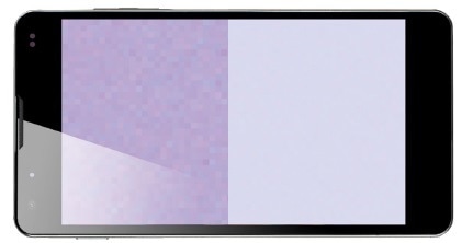
Figure 5. Results of the Radiant demura method for correction of emissive displays (like OLED, LED, and microLED), captured by a ProMetric® 29MP imaging system; before demura (left) and after (right).
The demura technique utilizes three individual steps:
- Quantification of every sub-pixel in the display to calculate the values of luminance at each pixel location (carried out on various test images to analyze different display colors) utilizing a high-resolution imaging colorimeter.
- Determination of the correction factors required to normalize any discrepancies in luminance between sub-pixels in the display employing the test analysis software.
- Application of correction factors to the display signals utilizing an external control IC (integrated circuit) system.
When an OLED display is fully assembled, test images can be presented on screen to the desired output color values.
These images allow for calibration and measurements to be computed for each of these values. For example, a ‘green screen’ with all green sub-pixels turned on can be employed as a sample image and the imaging colorimeter can analyze and note the brightness of every distinct green sub-pixel.
This is repeated for each primary color and, normally, white as well. This data can be collected during standard quality testing of the OLED display.
Determining the luminance values of each and every pixel in incredibly pixel-dense OLED displays can be difficult.
For standard Full High Definition (FHD, 1920 x 1080 pixel) and lower-resolution displays, a single 29-megapixel imaging system provides adequate resolution for testing.
For higher-resolution displays (such as the Quad High Definition or QHD), even incredibly high-resolution imaging systems may not be able to acquire all pixels in one image for a thorough analysis, particularly in the increasingly large displays of the present.
To solve this limitation and tailor a measurement technique for any arbitrary resolution and size of OLED display, Radiant’s demura technique uses a measurement system that combines data from a Spaced Pixel Test Pattern analysis, a patented technique (US Patent 9135851) that can be utilized with only one photometric imaging system
Figure 6. Example of the Spaced Pixel Test Pattern method of pixel-level luminance measurement for extremely high-resolution displays.
Dot matrix patterns of pixels are lit up at intervals and analyzed by the imaging system in several passes using a Spaced Pixel Test Pattern. Measurements are repeated for each dot-matrix pattern until every display pixel has been evaluated in its illuminated state.
When employing a camera with higher resolution than the display itself, every display pixel can be assessed over many image sensor pixels, allowing for the highest accuracy of the related pixel’s measured luminance value.
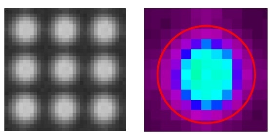
Figure 7. Each illuminated display pixel is automatically registered by the analysis software and defined within a region of interest (ROI). As the imaging system resolution is much higher than the display resolution, each display pixel may be measured across an ROI captured by multiple image sensor pixels.
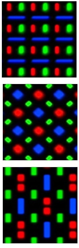
Figure 8. ROI are dynamically defined regardless of OLED pixel pentile structure, meaning that any arbitrary pixel pattern can be measured to apply demura to any display.
The software combines all images for measurement into one ‘synthetic image’ with an equal resolution to the measured display once all patterns of illuminated pixels have been analyzed.
This image presents each display pixel in columns and rows, enabling precise x,y coordinates for every pixel and their corresponding luminance values. This stage in the demura technique allows for the effective detection of defective pixels and their precise coordinates
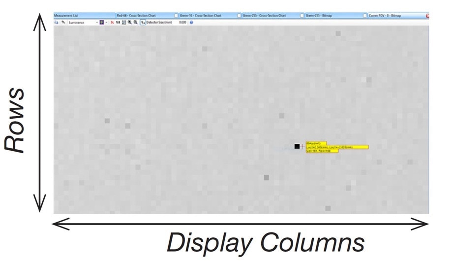
Figure 9. Software locates the defective pixels in the display using a synthetic image that combines the data from multiple high-resolution measurement images of the display.
Once these values have been established, special correction factors can be computed and applied to the electrical input of every specific sub-pixel, so that the brightness will be uniform and accurate throughout the complete display even at gray levels.
There is an extensive improvement in brightness, color, uniformity, and accuracy when this correction map is applied to the finished OLED display.
The total effect of demura is that displays that would have needed electronic compensation in order to pass quality inspection will now be able to pass which decreases waste and improves production yield.
The net effect of demura is that displays that would have needed electronic compensation in order to pass quality inspection will now be able to pass, decreasing waste and improving production yield.
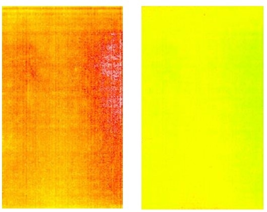
Figure 10. Captured images of a blue test screen on an OLED display before and after demura correction (shown using false color to illustrate luminance levels).
Radiant Vision Systems Solutions
OLED technology is proving to be the next generation for flat-panel displays and particularly curved displays, but technical challenges concerning production yields and image quality must be solved before OLED can be considered commercially viable outside of the smartphone market.
The challenges facing OLED manufacturers, while unique, are similar to the technical issues that have already been corrected by Radiant Vision Systems in LED screen manufacturers and LCD production.
ProMetric® Imaging Colorimeters
Radiant Vision Systems ProMetric Imaging Colorimeters are highly sensitive, highly precise, imaging systems calibrated to the same standards in the human visual perception of angular and spatial distributions of color and brightness (luminance).
Radiant Vision Systems provides 10 alternative models of imaging colorimeters, over twice as many as others in the industry, with several selections for sensitivity and resolution.
The optimal system for particular display testing applications will be reliant on the desired resolution requirements and measurement accuracy.
TrueTest™ Software
Precise measurement of OLED display performance is crucial, but the analysis of the measurement data is equally important.
Radiant Vision Systems TrueTest Automated Visual Inspection (AVI) Software completes the display test solution and makes data actionable through the implementation of test sequences against pass or fail criteria that is user-defined.
TrueTest is a software test sequencer and suite with integrated tests available for line defect detection, display uniformity testing, contrast measurement, pixel defect detection, and more.
TrueTest enables the user to choose from a test library and order tests in any sequence for the quick analysis of several features. The user can also determine the parameters of the test and the pass or fail criteria.
TrueMURA™ is an add-on test suite module to TrueTest that provides JND (‘just noticeable difference’) mura and blob analysis methods. TrueTest includes software alignment and moiré pattern removal functions to make test setup easier.
On the production line, it functions in Operator mode where access to test parameters is restricted, stopping any changes being made.
TrueTest also keeps test parameters, configuration information, and pass or fail criteria for several display models so that the proper data file can be changed or applied instantly during live production.
The challenges facing OLED manufacturers, while unique, are the same as technical issues that have already been corrected by Radiant Vision Systems in LED screen manufacturers and LCD production.
Integration and Support
The practical implementation of the Radiant Vision Systems display test solution needs both software and physical integration in the production line. Radiant Vision Systems is known for working with fixture providers selected by the customer, or offering complete turnkey solutions that include fixtures.
TrueTest software can function in a standalone mode, but more frequently it is integrated with the Production Control System (PCS) of the line of a manufacturer.
This integration can offer testing that is fully automated, wherein Radiant’s software is triggered by the PCS, or just allows a reporting interface for pass or fail results (and possibly testing data).
TrueTest can also be organized to work with barcode readers and video pattern generators (or similar). Radiant Vision Systems gives international support for all TrueTest and ProMetric solutions.
Its support staff gives installation, engineering, maintenance, training, and calibration services. Radiant Vision Systems has support colleagues in the US, China, Japan, Korea, and Europe, helping thousands of imaging colorimeters being deployed on hundreds of international production lines wor.
References and Further Reading
- DSCC. (2018, March). DSCC Releases Latest OLED Forecast. https://www.displaysupplychain.com/blog/dscc-releases-latest-oled-forecast

This information has been sourced, reviewed and adapted from materials provided by Konica Minolta Sensing Americas.
For more information on this source, please visit Konica Minolta Sensing Americas.