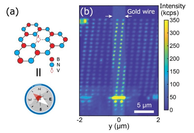
Quantum sensor nanoarray. (a) Boron vacancy defect in hexagonal boron nitride. The vacancy acts as an atom-sized quantum sensor for magnetic field measurements. The magnetic field-sensitive quantum sensor behaves like a nano-sized “magnetic needle”. (b) Photoluminescence of a quantum sensor nanoarray. By analyzing the change in the photoluminescence intensity in response to microwaves, the researchers measured the magnetic field at each sensor spot. Many quantum sensors are generated at each bright spot. Image Credit: The University of Tokyo
For instance, in reaction to a magnetic field, an atom modifies its spin, which has two possible values akin to a magnet’s poles. Superconductors and other quantum materials, as well as biomedical devices, can both benefit from the use of magnetic field sensors.
Using such an unprecedented sensor, we want to observe a microscopic world that no one has ever seen.
Kento Sasaki, Assistant Professor, University of Tokyo
The goal of the project was to create reliable quantum sensors that could be placed close to objects like disks and wires. To date, however, it has been difficult to precisely arrange atoms in a way that allows for the ability to detect minute fluctuations in the magnetic field.
Sasaki added, “Although individual quantum sensors are small, their spatial resolution is restricted by the distance between the sensor and the measurement target.”
The researchers developed a method for fabricating nanoscale quantum sensors on the measurement target’s surface to address the issue.
The researchers employed boron vacancies or lattice defects in two-dimensional hexagonal boron nitride, a thin crystalline substance having nitrogen and boron atoms, as quantum sensors. Since its discovery as a quantum spin sensor in 2020, the boron vacancy defect has been the new kid on the block.
The scientists removed the Scotch tape from the crystal to get a thin hexagonal boron nitride sheet. The thin layer was adhered to the target gold wire by the researchers. Then, they used a high-speed helium ion beam to blast the film, which caused boron atoms to escape and create the 100 nm2 boron vacancy spots.
Numerous atom-sized vacancies that behave like tiny magnetic needles are present in each spot. The sensors’ spatial resolution improves as the spots get closer to one another.
Based on the intensity of light emitted from the spots in the presence of microwaves, the team assessed the magnetic field at each place as the current flowed through the wire. The accuracy of the high-resolution quantum sensors, as demonstrated by the observed magnetic field values nearly matching the calculated values, astounded the researchers.
Even at room temperature, it is possible to detect the change in the sensor’s spin state caused by the presence of a magnetic field, making it simple to find the currents and magnetic field in the area.
Additionally, the van der Waals force is all that is needed for the boron nitride nanofilms to adhere to items, making it simple for the quantum sensors to adhere to various materials.
This method will be used by Sasaki and his team to study quantum materials and condensed matter physics.
“It will enable direct detection of the magnetic field from, for example, peculiar states at edges of graphene and microscopic quantum dots,” Sasaki stated.
Atomic-scale quantum sensors are beginning to transform how humans perceive microscopic surroundings and thus comprehend macroscopic features. Beyond basic science research, their applications are broad.
They can aid in mapping subsurface settings, imaging human brains, pinpointing geolocation, and detecting volcanic eruptions and geological movements. The use of Sasaki and his team’s nanoscale quantum sensors in superconductors, semiconductors, and magnetic materials is something they are eager to see.
The National Institute for Materials Science (NIMS), the National Institute of Advanced Industrial Science and Technology (AIST), and the University of Tokyo collaborated on this study.
Journal Reference
Sasaki, K., et al. (2023) Magnetic field imaging by hBN quantum sensor nanoarray. Applied Physics Letters. doi:10.1063/5.0147072.