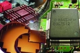
Product defects and quality issues can be caused by unidentified clamping forces in the process of computer chip and heat sink mounting or wafer probe testing. As a consequence, the yields may be lowered, and cost and production waste increased.
Solution
The I-Scan™ force and pressure mapping system is a key diagnostic and machine set-up tool for clamping fixtures. The sensors are ultra-thin (0.1 mm) and can be positioned between any two mating surfaces, for instance a heat sink and its heat source, or probe and wafer.
Real-time viewing is enabled by the system, which shows the distribution of the pressure between the clamping fixture and opposing surface.
In cases where the ideal pressure is not achieved, further adjustments can be made to optimize the clamping fixture design, quantify forces, or determine ideal protocols, for example torque patterns and procedures.
Optimization of the pressure distribution can also be achieved with the I-Scan pressure mapping system. This can be done before the testing sequence or production run so as to save precious company time and money.
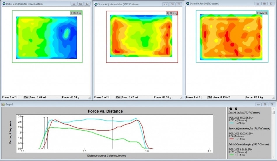
Progressive iterations of tooling, process, and/or fixturing adjustments yield more even pressure distribution across the area of interest.
Semiconductor Clamp Pressure distribution Applications
- Coplanarization
- Research and Development
- Before and after adjustment comparison
- Detect defects or obstructions
- Quality assurance testing
- Machine to machine comparison
- Design verification testing
Benefits of Pressure Mapping
- Better bonds and seals
- Identify low yield machines
- Manufacturing yields can be increased
- Costs and product waste can be reduced
- Less wear and tear on production equipment
- Provides data for improved design
- System Flexibility, it can adapt to different or changing measurement needs
Watch this video to learn more about how Pressure Mapping Technology can help validate component press fits or seals:
Pressure Mapping in R&D - Evaluating Component Press Fits & Seals

This information has been sourced, reviewed and adapted from materials provided by Tekscan, Inc.
For more information on this source, please visit Tekscan, Inc.