When creating components for integrated circuits or photovoltaic devices, it is important to have precisely-manufactured semiconductors and electronics. All steps in the fabrication process, including cleaning, etching, and polishing, need to be fine-tuned when the evenness of finished product is measured in microns.
The semiconductor industry is worth $300 billion and is still growing. As a result, throughput and costs have become driving factors in production, leading to larger wafers that have introduced new quality control challenges.
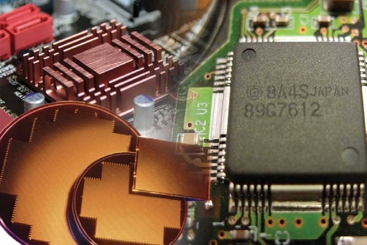
Electrical components are integrated to a printed circuit board (PCB), which means the functionality and performance is directly related to the reliability of connections. This is of crucial importance, as intermittent component connections can result in total failure. For example, a weak connection to a heat sink can lead to diminished performance or breakdown.
To make consistent, high-quality products, manufacturers and need designs and assembly processes that are reliable, particularly during automated processes. It is even more important for electronics producers to maintain quality in the communications era.
Semiconductor Applications Using Pressure Mapping
The following section reviews several common semiconductor applications and presents the information that a Tactile Pressure Mapping System can provide.
Heat Sink
High density, active electronics emit energy that can raise their temperature, lead to failures and decrease performance. For heat to be dissipated properly from the components it is secured to, there must be even contact between the part that is being cooled and the heat source. Only then will the heatsink be able to dissipate heat properly.
There needs to be a high and even pressure between the heat sink and the source for a proper thermal transfer to be achieved. The heat sink and the hard surfaces involved have a mechanically “stiff” nature, which can make thermal transfer harder to achieve. Even though contact can be achieved well at one or two points, larger regions of potential contact have gaps.
Validate Heat Sink and Mount Contact
During the mounting of a heat sink, uniform pressure distribution is vital. Pressure mapping during mounting enables the user to see the actual pressure distribution, along with any potential complications that may arise as a result from the weak and uneven contact pressure between the heat sink and the mount.
Heat Sink with Pressure Mapping Sensor
The image below shows a 2D display of the pressure of a heat sink. The right corner exhibits higher pressures, which indicates that the contact area between the heat sink and the heat source is not uniform. As a consequence, potential problems with cooling and performance may arise.
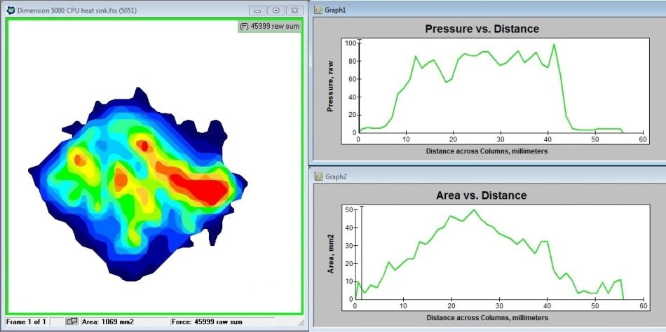
2D pressure display of a heat sink being mounted. Higher pressures are shown in red along the right corner, where the heat sink and source are not even.
The paper-thin sensors can be easily placed between the heat sink and the heat source to perform the evaluation, while minimally affecting the dynamics of the interface. It is possible to carry out measurements during the process of mounting a sink to see where the uneven pressures are located.
After that, it is possible to make adjustments to the heat sink and the heat source; these new measurements can be applied to achieve even contact. The design and assembly processes can be improved using pressure mapping with heat sinks. It can also minimize testing time for validation and reduce failures. This leads to improved reliability and yields.
CMP Wafer Polishing
In chemical mechanical polishing (CMP) systems, a crucial step in the semiconductor process is the characterization and parallelism of polishing heads. If the polishing head is not suitably conditioned with a consistent roughness, it can leave behind particle residue.
CMP is a crucial manufacturing process in the semiconductor industry. Improving non-uniformity during the polishing process is the main goal of manufacturers. An uneven polishing head can cause cracks in the wafer, thus, leading to product waste.
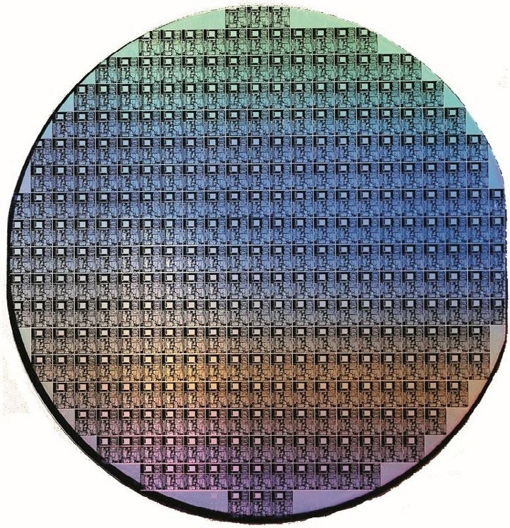
Semiconductor Wafer
Pressure Mapping Shows Parallelism of CMP Wafer
It is possible to measure the pressure distribution during the various stages of CMP wafer polishing using pressure mapping. To measure the pressure distribution along the entire wafer, in real time, the pressure mapping sensors of Tekscan can be integrated into the CMP polishing machine. The software can display any problems with pressure variations or parallelism that may have arisen during the polishing process. To ensure an even pressure, it is then possible to make machine adjustments and take new measurements.
The figure below shows a pressure distribution during wafer polishing that is not uniform, with higher pressure being applied to the two lobes of the polishing head. The uneven pressure on the wafer from the polishing head is probably the result of a material being removed.
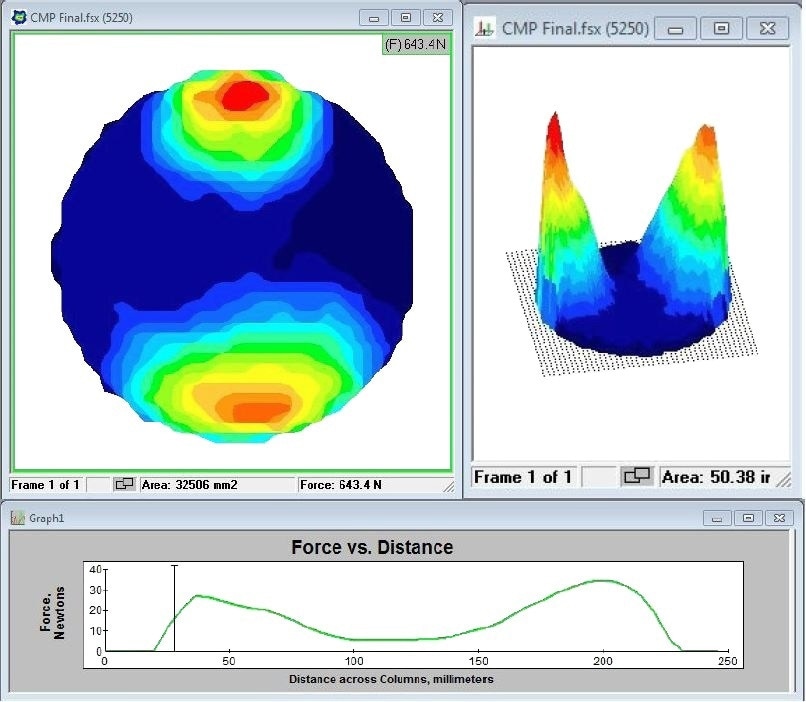
2D and 3D pressure display of Semiconductor Wafer Polishing. Higher pressures are shown on the two lobes of the polishing head indicating uneven pressures being put on the wafer from the polishing head.
Wafer Bonding
In CMP systems, equipment state measurements, such as characterization and parallelism of polishing heads, are a crucial step in the semiconductor process. Particle residue will be left behind if the polishing head is not suitably conditioned with a consistent roughness.
CMP is a crucial manufacturing process in the semiconductor industry. A key goal for manufacturers of wafers is to improve quality during the polishing process. An uneven polishing head can cause cracks in the wafer and create product waste.
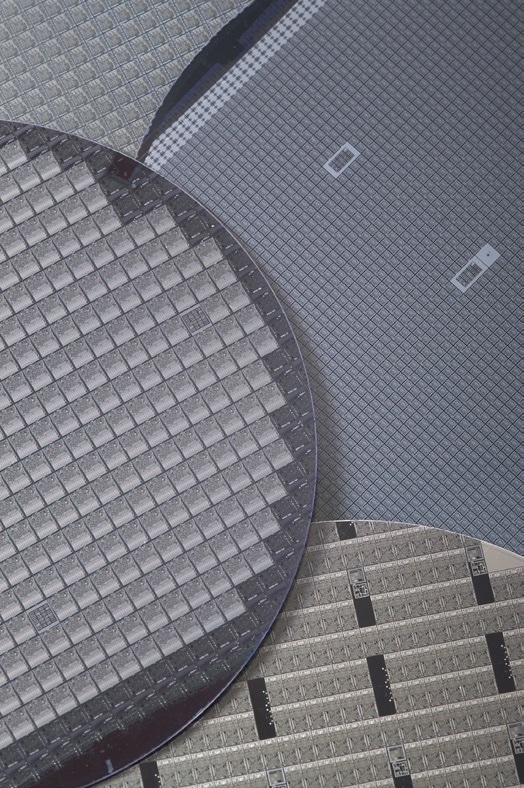
Semiconductor Wafers
Pressure Mapping Shows Parallelism of CMP Wafer
It is possible to measure the pressure distribution during the various stages of CMP wafer polishing using pressure mapping. To measure the pressure distribution along the entire wafer, in real time, the pressure mapping sensors of Tekscan can be integrated into the CMP polishing machine. The software can display any problems with pressure variations or parallelism that may have arisen during the polishing process. To ensure an even pressure, it is then possible to make machine adjustments and take new measurements.
The figure below shows a pressure distribution during wafer polishing that is not uniform, with higher pressure being applied to the two lobes of the polishing head. The uneven pressure on the wafer from the polishing head is probably the result of a material being removed.
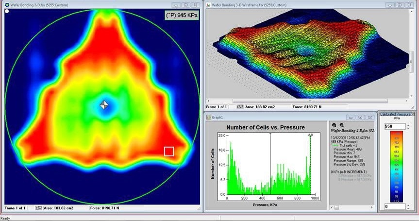
2D and 3D pressure display of Semiconductor Wafer Bonding. Higher pressures are shown in red, indicating uneven pressures being put on the wafer from the bonding process.
Post-CMP PVA Brush Testing
Polyvinyl alcohol (PVA) brushes are used in the semiconductor process during the post-CMP cleaning stage. During the process of PVA brushing, post-CMP cleaning particle removal is conducted through direct contact between the soft PVA brush and the wafer surface. The brush asperities absorb the wafer surface contamination, while the brush rotates to remove the particles from the wafer.
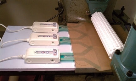
PVA Brush Roller over Pressure Mapping Sensors
Proper Brush-to-Wafer Contact Pressure with Pressure Mapping
Ensuring proper brush-to-wafer contact pressure and contact area is crucial in achieving clean and particle-free wafers. Pressure mapping and tactile pressure sensors provide instant feedback and indicate how effective the brush is.
For this to be possible, the distribution of pressure and area in real-time is measured. If any inconsistencies in pressure could potentially cause particles not to be removed from the wafer, they are displayed by the pressure mapping software.
The image below shows 2D and 3D displays of the pressure output of a PVA Brush roller used during the semiconductor wafer post-CMP process. Uneven pressures were clearly highlighted along the middle of the brush. Information like this can be utilized to help designers adjust the brush to fix the pressure distribution and make it more even. New measurements can be taken to ensure an even contact pressure across the entire brush.
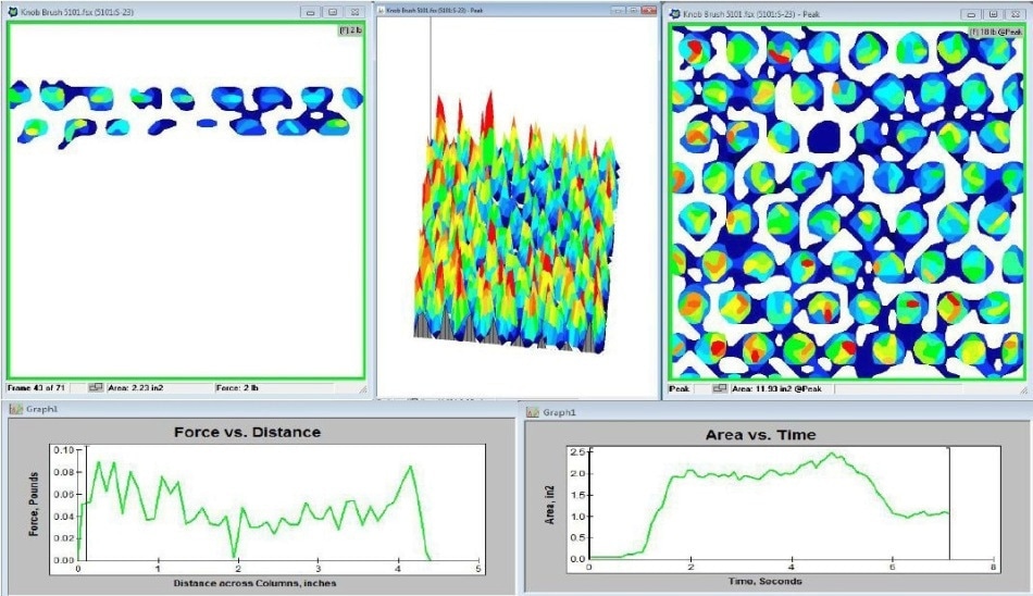
2D and 3D pressure display of a PVA Brush Roller. Uneven pressures are clearly evident
along the middle of the brush where more pressure is being applied.
Utilizing pressure mapping during post-CMP PVA brush process helps to ensure a consistent wafer cleaning performance and improved consistency, which helps reduce machine set-up time and increase product yields.
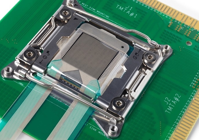
Precision Clamping
During computer chip and heat sink mounting or wafer probe testing, it is possible to have unknown forces that cause significant product defects and issues with quality. This can lead to lower yields, increased costs and, ultimately, product waste.
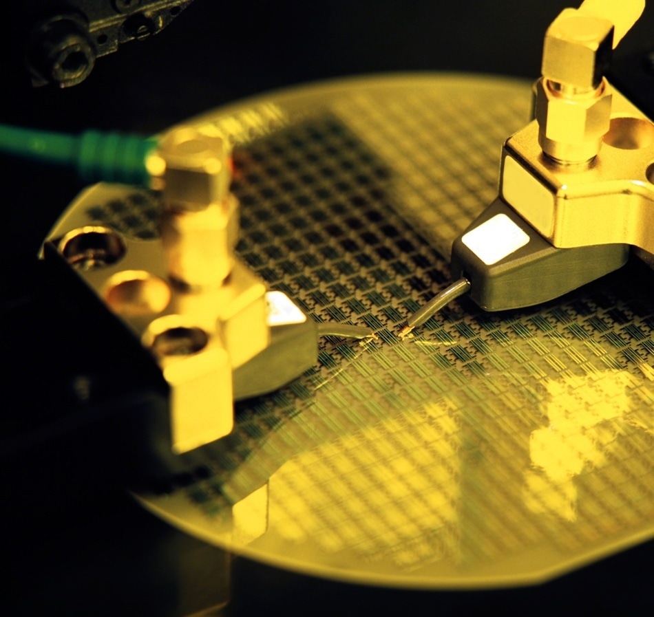
Semiconductor Precision Clamping
Evaluate Pressure Distribution During the Entire Clamping Process
Pressure Mapping is a key diagnostic and machine set-up tool that can be used for clamping fixtures. Ultra-thin sensors can be placed between any two mating surfaces, such as an integrated circuit on a PCB, or a probe and wafer. Pressure mapping makes it possible to take both static and dynamic pressure impressions before, during, and after machine adjustments. This allows the user to see how the changes in pressure can affect planarization and contact area.
Measuring these key process steps and equipment states enables engineers and machine operators to establish product quality standards.
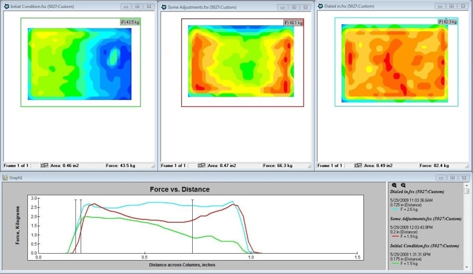
Progressive iterations of tooling, process, and/or fixturing adjustments, yield more even pressure distribution across the area of interest.
If an optimal pressure is not achieved, adjustments can be made to optimize the clamping fixture design, quantify forces, and determine ideal protocols (such as torque patterns and procedures). Optimizing pressure distribution before a testing sequence of the production run is also possible with pressure mapping, which helps save precious company time and money.

This information has been sourced, reviewed and adapted from materials provided by Tekscan, Inc.
For more information on this source, please visit Tekscan, Inc.