Zinc oxide (ZnO) is an interesting substitute for wide bandgap semiconductors, showing promising applications in flexible electronics and sensors.
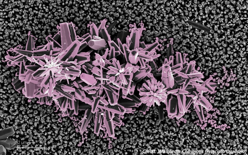
Image Credit: Wikimedia Commons (Principia Dardano)
Plasma treatment can be used to create surfaces for ZnO deposition, enhance electrical properties through organic impurity elimination and surface alteration, and simplify the fabrication of ZnO-based devices.
Introduction
ZnO is a wide bandgap semiconductor, with electrical and physical properties similar to that of GaN III-V semiconductor.
Due to the abundant availability of zinc and the capability to deposit ZnO at low temperatures, ZnO provides a cost-effective alternative to GaN for applications like optoelectronics, light-emitting diodes (LEDs), and flexible electronics.1-3
ZnO shows optical transparency in the visible spectrum and, with suitable doping, can be tuned to possess high conductivity. Consequently, ZnO is additionally attractive as a low-cost alternative to indium tin oxide (ITO), a transparent conducting oxide, or as the semiconducting layer in thin film transistors (TFTs).
Various methods, such as sputtering or spin coating from solution, can be used to deposit ZnO films. However, the as-deposited ZnO films generally necessitate additional processing to produce the necessary electrical properties for optimal device performance.
This article explores numerous research studies that employed plasma treatment to induce oxygen vacancies and modify ZnO surface chemistry, aiming to create ZnO-based sensors and thin TFTs with enhanced electrical properties and device performance.
Zinc Oxide for Sensors
Sensors need high surface activity (active sites) to identify the target analyte with adequate sensitivity. Plasma treatment modifies ZnO surface morphology and generates oxygen vacancies, resulting in oxygen-deficient ZnO which functions as active sites for gas or chemical detection, thereby enhancing sensor performance.
Oxygen vacancies on semiconductors can influence gas adsorption by increasing carrier concentration through the formation of unpaired electrons and adjusting the energy band structure (decreasing the energy band gap in some instances), leading to enhanced sensing and increased electron transfer.
Increasing the oxygen vacancies raises the concentration of adsorbed oxygen species on the surface, producing more unpaired electrons and active sites. This, in turn, facilitates gas molecule adsorption and redox reactions, amplifying the sensor’s signal response.
Using the Basic Plasma Cleaner, Li et al. applied Ar plasma on annealed ZnO films to create a ZnO-based metal oxide semiconductor (MOS) gas sensor for triethylamine (TEA) detection. Triethylamine is a frequently utilized organic solvent in chemical synthesis which can be damaging to aquatic and human life when released into waste streams.
The researchers stimulated the assembly of oxygen vacancies by changing the Ar plasma treatment time (1-10 minutes), thus increasing the electrical resistance signal response of the sensor.
Their XPS measurements and spectral analysis revealed that a 5-minute exposure to Ar plasma created the greatest oxygen vacancy content in plasma-treated ZnO films (shown in Figure 1). The 5-minute Ar plasma treatment also produced ZnO-based gas sensors with optimal performance at 250 °C.
These sensors demonstrated a moderately high response signal (ratio of electrical resistance with TEA to the baseline resistance without TEA), fast response and recovery time, and notable selectivity for 10 ppm TEA (against other organic solvents).
By measuring the sensor’s response signal over numerous TEA concentrations (1-100 ppm), the researchers derived a potential limit of detection of approximately 22 ppb, suggesting the capability to identify low levels of TEA. Their work showcased a potential approach for fabricating affordable MOS gas sensors for organic amines detection.
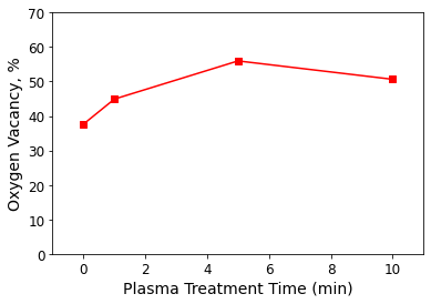
Figure 1. Oxygen vacancy content with plasma treatment time of ZnO films annealed at 700 °C for 2 hours followed by Ar plasma treatment. Data from Li Z, Liu X, Zhou M, Zhang S, Cao S, Lei G, Lou C and Zhang J. J. Hazard. Mater. (2021) 415: 125757. DOI: 10.1016/j.jhazmat.2021.125757
In a separate investigation, Perera et al. developed a sensor for human biomarker identification based on oxygen-deficient ZnO films. Their sensor utilized human saliva and sweat as the analyte, with cardiac inflammatory biomarkers C-reactive protein (CRP) and interleukin 6 (IL-6) chosen as the model antigen.
Oxygen-deficient ZnO is preferred due to the abundance of loosely bound oxygen, providing additional opportunities for surface functionalization, and creating active sites for biosensing. Additionally, (3-glycidyloxypropyl)trimethoxysilane (GPS) was incorporated as a crucial functional layer in the device.
GPS enables the attachment and orientation of antibodies so that their antigen-binding sites protrude from the surface. This increases the exposure to incoming antigens and enables maximal antigen binding.
The sensor was fabricated by sputter deposition of an oxygen-deficient ZnO film onto an oxidized silicon substrate, followed by deposition of Au/Cr electrodes to quantity electrical resistance across the exposed ZnO surface.
O2 plasma was applied in the Expanded Plasma Cleaner to as-sputtered ZnO to eliminate organic impurities and present oxygen-containing hydroxyl groups, enhancing GPS binding to the surface. The water contact angle of as-deposited ZnO declined from approximately 73° to under 5° after a 10-minute exposure to O2 plasma.
According to the authors, the surface hydroxyl groups establish covalent bonds with the silicon in GPS silane. This facilitates the epoxy group of GPS to readily bind to the amine group of an incoming antibody.
The resultant sensor measured the difference in electrical resistance between an antigen-bound surface and an as-prepared surface. The percentage change in electrical resistance (ΔR, %) indicates the antigen concentration bound to the surface. The measured ΔR was proportional to IL-6 and CRP antigen concentration.
The device demonstrated a comparatively fast incubation period, where ΔR stabilized within 10 minutes of exposure to the analyte. This suggests optimal immobilization times of 10 minutes for both antigens.
The effective demonstration of the ZnO biosensor in identifying IL-6 and CRP provides promise that other antigen-specific devices can also be fabricated with a suitable selection of functionalized layers and antibodies to the target antigen to illicit appropriate antibody/antigen interactions.
Zinc Oxide Thin Film Transistors
Meena et al. devised a solution-cast ZnO as the charge transport and semiconducting (channel) layer in TFTs constructed on flexible polyimide (PI) substrates. Their research concentrated on utilizing low-power O2 plasma to regulate oxygen vacancies in ZnO and enhance carrier concentration and charge carrier mobility.
The fabrication process involved spin-coating ZnO from a zinc acetate precursor solution, followed by O2 plasma treatment at changing times (1-5 minutes) and succeeding thermal annealing at 250 °C for 1 hour to passivate the surface.
The treatment with plasma eliminated organic impurities and produced oxygen vacancies to further provide free charge carriers.
AFM imaging demonstrated that plasma-treated ZnO films were comparatively smooth (1-2 nm RMS surface roughness) with a continuous (crack-free) surface. Optical transmittance spectra displayed that plasma-treated ZnO on PI substrates maintained a transmittance of 80-85 % in the visible spectrum.
XPS spectra revealed a shift in the native carbon C-C peak linked with the underlying PI substrate. FTIR spectra revealed a constant decrease and subsequent absence of absorbance bands connected with volatile organic groups.
Both spectra indicated that O2 plasma effectively eliminated loosely bound carbon layers and organic impurities. Based on this, the authors suggested the exclusion of acetate groups from the zinc acetate precursor and the subsequent creation of ZnO.
Electrical measurements were conducted on the TFTs using plasma-treated ZnO as the channel layer.
The drain current versus gate voltage (ID-IG) curves were analyzed, and the field effect carrier mobility and carrier concentration were extracted for changing plasma treatment times (shown in Figure 2).
Notably, both mobility and carrier concentration reached their peak at a 2-minute plasma exposure and steadily declined with prolonged plasma treatment (up to 5 minutes).
The researchers suggested that a brief plasma exposure was effective in eliminating organic impurities (such as acetate precursor) and creating surplus oxygen vacancies. This provided free electrons for conduction in the ZnO channel layer, leading to an increase in charge carrier mobility.
They proposed that the subsequent decline in mobility and carrier concentration was linked to a reduction in oxygen vacancies with prolonged plasma exposure. Reactive oxygen species from O2 plasma can fill oxygen vacancies, capturing free electrons and thereby reducing the supply of charge carriers.
Their research concluded that short plasma treatments of up to 3 minutes were optimal to augment ZnO electrical properties, showcasing the feasibility of using low-temperature fabrication methods for developing TFTs on flexible substrates.
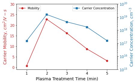
Figure 2. Charge carrier mobility and carrier concentration as a function of O2 plasma treatment time in plasma-treated ZnO-based thin film transistors on flexible polyimide substrate. Data from Meena JS, Chu M-C, Chang Y-C, You H-C, Singh R, Liu P-T, Shieh H-PD, Chang F-C and Ko F-H. J. Mater. Chem. C (2013) 1(40): 6613-6622. DOI: 10.1039/C3TC31320D
References and Further Reading
Relevant Articles from Harrick Plasma Users
- Li Z, Liu X, Zhou M, Zhang S, Cao S, Lei G, Lou C, and Zhang J. “Plasma-induced oxygen vacancies enabled ultrathin ZnO films for highly sensitive detection of triethylamine.” J. Hazard. Mater. (2021) 415: 125757. DOI: 1016/j.jhazmat.2021.125757
- Perera GS, Ahmed T, Heiss L, Walia S, Bhaskaran M, and Sriram S. “Rapid and Selective Biomarker Detection with Conductometric Sensors.” Small (2021) 17: 2005582:1-12. DOI: 1002/smll.202005582
- Meena JS, Chu M-C, Chang Y-C, You H-C, Singh R, Liu P-T, Shieh H-PD, Chang F-C and Ko F-H. “Effect of oxygen plasma on the surface states of ZnO films used to produce thin-film transistors on soft plastic sheets”. J. Mater. Chem. C (2013) 1(40): 6613-6622. DOI: 1039/C3TC31320D
Supplemental References (Do not Report Using Harrick Plasma Instruments)
- Kołodziejczak-Radzimska A and Jesionowski T. “Zinc Oxide – From Synthesis to Application: A Review.” Materials (2014) 7: 2833-2881.
- Janotti A and Van de Walle CG. “Fundamentals of zinc oxide as a semiconductor.” Rep. Prog. Phys. (2009) 72: 126501.
- Borysiewicz MA. “ZnO as a Functional Material, a Review” Crystals (2019) 9: 505.

This information has been sourced, reviewed, and adapted from materials provided by Harrick Plasma.
For more information on this source, please visit Harrick Plasma.