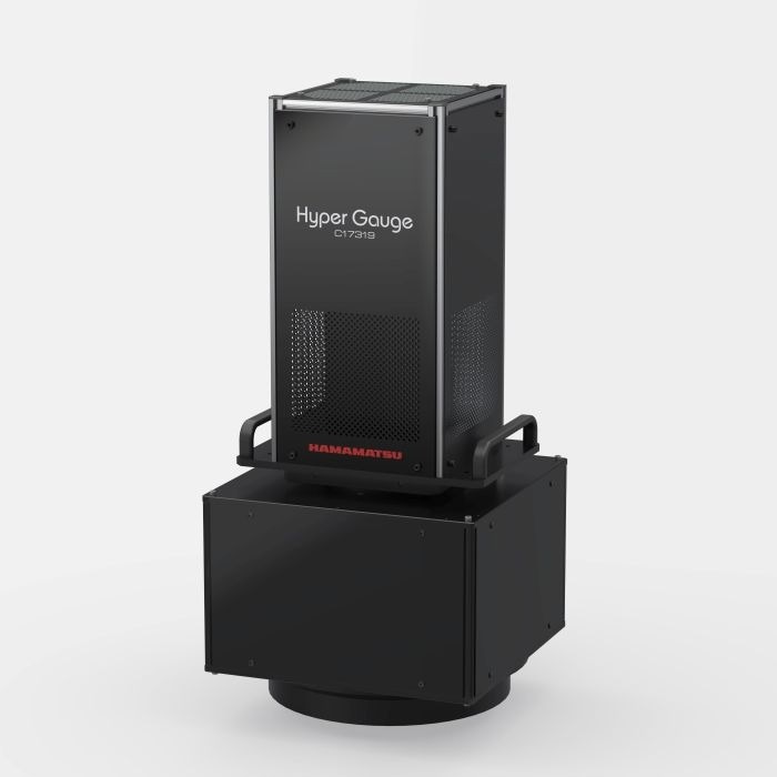
Hamamatsu Photonics has developed the HyperGauge thickness measurement system C17319-11, a new device designed to enhance productivity in semiconductor manufacturing processes. It features our proprietary wavelength detection technology, “λ-Capture®,” which uses a high-sensitivity camera to enable full-surface measurement of wafers up to 300 mm in diameter in just 5 seconds.
 HyperGauge In-plane Film Thickness Meter C17319-11. Image Credit: ©Hamamatsu Photonics
Key Benefits
Designed for both bare and patterned wafer inspection, the device delivers high resolution and excellent measurement reproducibility, essential for reducing process losses and improving yield in semiconductor manufacturing. It supports a wide range of applications from observing full-surface thickness distribution on irregular or ultra-thin wafers to evaluating structures on patterned wafers. When integrated into semiconductor manufacturing equipment, it enables efficient film-thickness inspection at each process stage, strengthening both productivity and quality.
Key benefits include:
- High Resolution & Reproducibility: Ensures accurate inspection for both bare and patterned wafers.
- Wide Application Range: Observes full-surface thickness distribution and evaluates patterned wafer structures.
- Process Efficiency: Reduces process losses and improves yield through efficient film-thickness inspection at each stage.
- Proven Performance: Highly rated by major domestic semiconductor manufacturers for its new “snapshotting in-plane film thickness distribution” concept and overall performance.
Product Overview & Features
This product is a device that measures wafer film thickness in two dimensions using a high-sensitivity camera. Wafer mapping is performed simultaneously with film thickness measurement. This makes it easier to select measurement locations and align positions compared to point sensor methods, while also enabling rapid acquisition of thickness distribution.
Features include:
- High-speed measurement: Acquire thickness distribution in just 5 seconds
- High resolution: Detailed measurement with 0.3 mm accuracy
- No moving parts: Minimizes risk of particle generation
- Easy detection of specific points: Facilitates measurement of desired wafer locations compared to point sensor methods
- Equipped with proprietary “λ-Capture” technology: New film thickness measurement method achieves both accuracy and reproducibility