Sensors are devices, modules or subsystems that are capable of detecting and responding to a certain type of input that has been acquired from the physical environment1. The perceived input can range from light, heat motion, moisture, pressure and various other physical phenomena that regularly occur in the environment surrounding the instrument.
The sensor then transmits the information it has received and subsequently provides an output as a general signal. This signal is then converted to a human readable display, or, in some cases, the information can be further transmitted electronically over a network for reading or further processing.
The simplest example of a sensor that we commonly see is a motion sensor1. Motion sensors function by transmitting energy in the form of microwaves, ultrasonic waves or light beams. This energy is then detected by the sensor when the flow of energy is interrupted by something that enters its path1.
The Evolution of Image Sensors
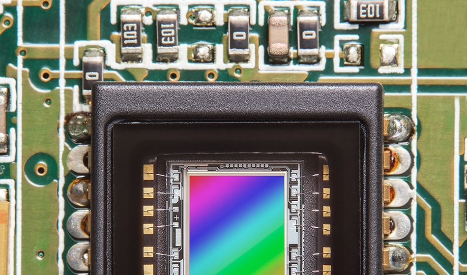
ASB63 / Shutterstock
The evolution of many types of audio and video electronic devices has been realized as a result of growing advancements within the semiconductor industry2. The enhanced memory and high-speed data processing capabilities of modern digital cameras, for example, can be directly attributed to the progress in the semiconductor industry that has transformed the electronics and engineering sectors over the last few decades. From the moment that charged coupled devices (CCD) were invented at Bell laboratories in 1969, several industries and laboratories have incorporated this technology for use in digital cameras2.
CCD sensors have significantly contributed in miniaturizing the size of the cameras, while also offering a smaller pixel size, greater resolution and excellent image quality. While this progress is evident, the trend in image sensors has slowly shifted to complementary metal oxide semiconductor (CMOS) sensors, as a result of the sensors’ ability to offer users with significantly faster capture speeds and a greater quality via high definition (HD) images 2. This transition in technologies has led to a boom in the digital camera market. For example, CMOS sensors are currently used extensively within the current generation of smartphones to capture photos. Furthermore, CMOS sensors have also led to the development of small-size HD video cameras2.
Challenges of Image Sensor Development
While digital cameras based on CMOS sensor technology have given users great benefits like system integration, low power consumption and ease of use, they do exhibit certain disadvantages, some of which include increased noise and reduced sensitivity2. Since most modern smart phones, video cameras and D-SLR cameras are based on CMOS sensors, the biggest challenge in these image sensors is attributed to the need to overcome the disadvantages of CMOS sensors and develop cameras that exceed human vision2.
The use of thin copper (Cu) wires rather than aluminum (Al) allows CMOS sensors to capture light in a more efficient manner while also facilitating the use of higher zoom lens2. Two dimensional (2D) materials, like graphene, may also be used as semiconductors in the future to create the next generation of image sensors. Once this transition to 2D materials occurs for these specific applications, an even greater range of possibilities will become available for the development of image sensors and electronics.
Potential Applications of Graphene Electronic Sensors
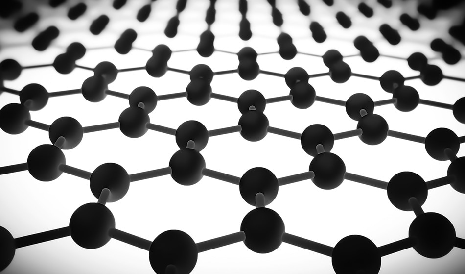
GiroScience / Shutterstock
As a result of graphene’s exceptional physicochemical and electronic properties, this material can be used during the development of a wide range of sensors including biological, mechanical and chemical sensors3. Some of the graphene-based biological sensors that have been developed with this material include:
- Glucose sensors based on reduced graphene oxide
- DNA sensors used for superior sensitivity and selectivity of nucleobases, nucleotides and single stranded DNA (ssDNA) and double stranded DNA (ds DNA)
- Graphene FET (GEFT) sensors used for the detection of DNA molecules
- Protein detection sensors
- Cellular detection and quantification sensors3.
Additional examples of mechanical sensors based on graphene include strain sensors and graphene-based chemical sensors, such as those capable of detecting the presence of combustible, flammable and toxic gases within a given area3.
Challenges Posing Graphene-Based Sensors
To better use the sensor in its appropriate environment, integrating sensors into sensor-based systems is essential. Despite this, graphene is currently used predominantly in sensors and not in sensing systems or smart sensors3. The extraordinary properties of graphene make it an ideal candidate that can be used as a multi-use sensor, such as a single sensor that is required to simultaneously measure strain, pressure and magnetic field3. The development of these types of multiuse sensors and sensing systems based on graphene is expected to have a wide array of consumer applications3.
References
- “Sensor” – WhatIs.com
- “Challenges of Image-Sensor Development” – IEEE Xplore
- “Graphene electronic sensors – review of recent developments and future challenges” – IEEE Xplore
Disclaimer: The views expressed here are those of the author expressed in their private capacity and do not necessarily represent the views of AZoM.com Limited T/A AZoNetwork the owner and operator of this website. This disclaimer forms part of the Terms and conditions of use of this website.