Image Credit: Isuaneye/Shutterstock.com
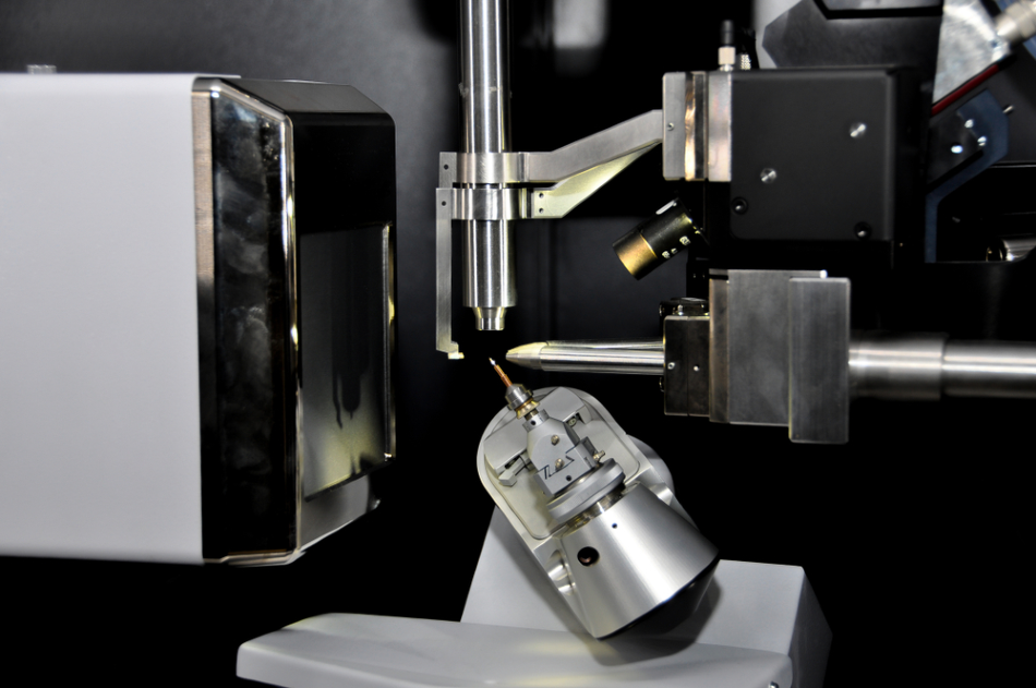
Charge-coupled devices (CCD) represent a major technology for digital imaging and has applications in astrophotography, spectrometers, and interferometers. The technique allows for light detection and is widely used in image sensing in professional, medical, and scientific applications where high-quality image data is necessary, such as digital cameras and active pixel sensors. CCD-based detectors allow scientists to record the best possible data under a given set of experimental conditions.
What is a Charge-Coupled Device?
A CCD is a charge-coupled device; it’s essentially an integrated circuit imprinted onto a silicon surface forming light-sensitive elements called pixels. They can digitally capture photons to generate an image of a sample and are basically doped silicon wafers, stamped with photoactive regions to capture photons.
These photoactive regions are based on a metal-oxide-semiconductor (MOS) structure, with MOS capacitors being the most basic of building blocks. Each of these capacitors acts as a photodiode, which in turn behaves as a pixel.
These p-doped metal MOS capacitors are biased above the threshold for inversion when image capture occurs. This allows for the conversion of incoming photons into electrons at the semi-conductor-oxide interface. The CCD is then used to read out these charges.
MOS technology was developed by Mohamed M Atalla and Dawon Kahng at Bell Labs in 1959. By the late 1960s, Willard Boyle and George E Smith, also of Bell Labs, realized CCD by creating a series of MOS capacitors in a row and stepped the voltage along one by one.
Their aim was to transfer charge along the surface of the semiconductor from one storage capacitor to the next. They were awarded the Nobel Prize in Physics in 2009 for this work and are among numerous Nobel Laureates from Bell Labs.
How a CCD Works
CCDs move electrical charge by ‘shifting’ the signal between stages within the device, one at a time. Charge is shifted between capacitive ‘bins’ in the device, to where the charge can be manipulated by converting it into a digital value, for example.
Its first experimental application was in image sensor technology, where a depleted MOS detector was utilized as a photodetector. In CCDs for capturing images, an image is projected through a lens onto a capacitor region, a photoactive area consisting of an epitaxial layer of silicon. This causes each capacitor to accumulate an electric charge proportional to the light intensity at that location.
A transmission region – technically the CCD – is made out of the shift register; once the array is exposed to an image, the control circuit causes each capacitor to transfer its contents to its neighbor (operating as a shift register). The last capacitor in the array offloads its charge into a charge amplifier, which converts this into a voltage.
CCD Use in Crystallography
Crystallography is an experimental science that determines the arrangement of atoms in crystalline solids; x-ray crystallography, for example, resolves the structure of large biomolecules like proteins. The method depends on the analysis of diffraction patterns of a sample targeted by a beam, be it X-ray, electrons or neutrons (the latter being known as electron or neutron diffraction).
In general, CCD detectors allow the user to examine the acquired diffraction image within seconds of recording the exposure. A typical CCD-based X-ray detector has a thin phosphor screen, which converts X-rays to visible light. It is coupled via lenses, image intensifiers and/or fiber optics to a CCD which records the light signal. There are several configurations of these basic components, the differences in which distinguish different CCD-based detectors.
The technique might be used for high-resolution data collection, difference Fourier analysis of enzyme complexes, solution of new structures using multiple isomorphous replacements and multiple-wavelength anomalous-diffraction phasing experiments.
For x-ray crystallography, the performance of CCD-based detectors is demonstrated using an expression that describes both the detector and the experiment. The detectors consist of an array of identical modules, each of which contains a phosphor X-ray-to-light convertor, a fiberoptic taper (normally used to maximize detector sensitivity and readout speed), and a CCD.
The performance is categorized by the detective quantum efficiency (DQE) and dynamic range (DR), and by four additional expressions: the detective collective efficiency (DCE); experimental detective quantum efficiency (XDQE); experimental detective collection efficiency (XDCE); and experimental dynamic range (XDR).
These additional expressions provide a way to include experimental constraints in the design of the detector, such as requirements to integrate Bragg peaks to maximum precision, and efficiently collect data to high resolution.
CCD detectors have become routine tools for X-ray diffraction structure determinations, they are increasingly available in X-ray laboratories and are also more often applied in high-pressure studies.
Advantages of CCD-Based Detectors
CCD image sensors became dominant, primarily because they deliver much more superior images with the fabrication technology available. CCD-based detectors are better than film and storage phosphor imaging plates in terms of performance and convenience. They can also collect data much quicker than other methods and offer a faster read-out. Other advantages include lower noise and higher efficiency; improved point spread function; negligible spatial distortion; and simpler engineering.
References and Further Reading
Disclaimer: The views expressed here are those of the author expressed in their private capacity and do not necessarily represent the views of AZoM.com Limited T/A AZoNetwork the owner and operator of this website. This disclaimer forms part of the Terms and conditions of use of this website.