Albert Einstein’s legacy expands further than the renowned theory of relativity and the ubiquitous equation E=mc². Many will credit his Nobel Prize in Physics to these achievements; however, the accolade was offered due to his groundbreaking explanation of the photoelectric effect. It may seem a minor discovery, but it has widespread implications in our everyday lives, impacting technologies typically taken for granted, including digital cameras and facial recognition systems used on smartphones and automation using LiDAR technology.
Understanding the Photoelectric Effect
Einstein’s experiment demonstrated that light comprises discrete energy packets called photons. When light of certain frequencies hits a metal surface, it liberates electrons, offering compelling evidence of light's particle nature. This discovery has immense implications, particularly in how we use the photoelectric effect in modern technology.
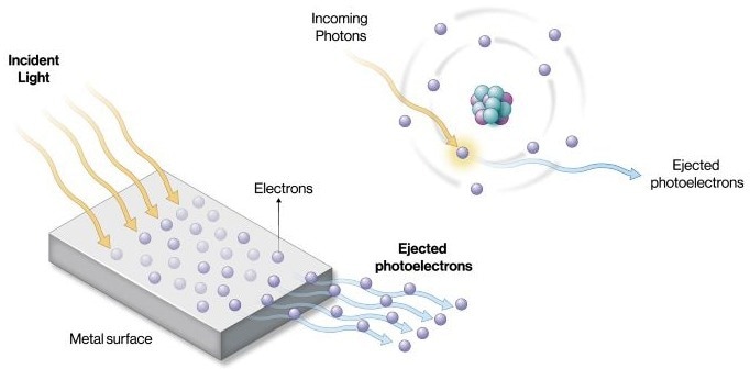
Image Credit: Hamamatsu Photonics Europe
LiDAR and TOF: Applications in Automation
Commonly accepted applications of the photoelectric effect are seen in acquisition systems for digital images, such as those found in digital cameras and facial recognition technologies.
These systems use the principles of light emission and detection discovered in Einstein’s findings. They significantly increase our ability to capture and understand visual data in real-time, an integral part of modern smartphone functionality.
The photoelectric effect also plays a critical role in identifying objects and people at various distances, allowing for automation features such as touchless doors and robotic obstacle avoidance. These applications utilize Light Detection and Ranging (LiDAR) technology, specifically the Time-of-Flight (ToF) method.
LiDAR Technology: A Detailed Overview
The guiding principle of TOF LiDAR is simple: a light source emits a concentrated light beam that reflects off an obstacle, such as a pedestrian or a vehicle, and bounces back to a photosensor. The sensor calculates the distance of the object, using the time it takes for the reflected light to reach it (Figure 1).
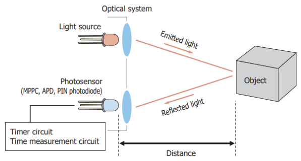
Figure 1. Basic principle of TOF LiDAR. Image Credit: Hamamatsu Photonics Europe
Light Sources in LiDAR Systems
A variety of light sources can be used in LiDAR systems, with the Pulse-Laser Diode (PLD) proving especially effective because of its high peak power under pulsed operation.
When choosing the ideal light source for applications, other parameters must be considered besides power. Factors such as electrical-to-optical conversion efficiency and the near-field pattern (NFP) are crucial. For example, Hamamatsu Photonics has PLDs with uniform light intensity (without temperature dependence) and high efficiency, which is critical for ensuring accuracy in distance measurements.
Hamamatsu offers an array of PLDs with a range of peak output power and emission widths. These light sources can be utilized for distance measurements, including hazard monitoring and laser radar in security applications.
In addition to standard products, a number of dedicated products are also available, including PLDs with vertical emission and PLDs with an integrated driver (including FET driver and capacitors), known as micro-High Speed Pulse Laser modules (µ-HPL).
The Heart of LiDAR Technology: Photosensors
A photosensor converts light into an electrical signal based on the photoelectric effect. There are numerous types, each with specific characteristics that help it fit the requirements, based on distance and measurement accuracy.
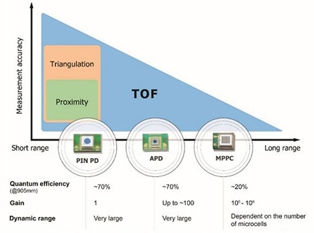
Figure 2. Types of detectors for TOF requirements. Image Credit: Hamamatsu Photonics Europe
Silicon PIN Photodiode (PIN PD)
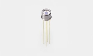
Image Credit: Hamamatsu Photonics Europe
The most commonly used and simple photosensor with high quantum efficiency and without any amplification, this works best for short-range detection because of its lack of gain.
Silicon Avalanche Photodiodes (APD)
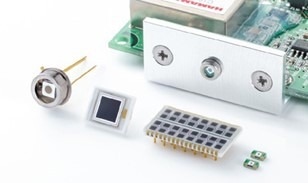
Image Credit: Hamamatsu Photonics Europe
When expanding the detection range, sensors with higher gain, such as the Si Avalanche photodiodes (APD), are crucial. They enable detection in low-light conditions and increase detection speeds.
Multi-Pixel Photon Counters® (MPPC®)
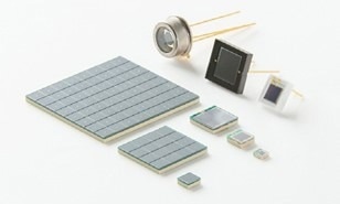
Image Credit: Hamamatsu Photonics Europe
Also called Silicon Photon Multipliers (SiPMs) or Single Photon Avalanche Diodes (SPADs), these devices are utilized for applications that require the detection of single photons with a high gain or that are in very low light levels while minimizing noise.
How do SPADs work?
When a reverse bias voltage greater than the APD’s breakdown voltage is applied, technically referred to as operating the APD in a breakdown state, this is Geiger-mode operation. As demonstrated in Figure 3, a very high gain can be reached in this state.
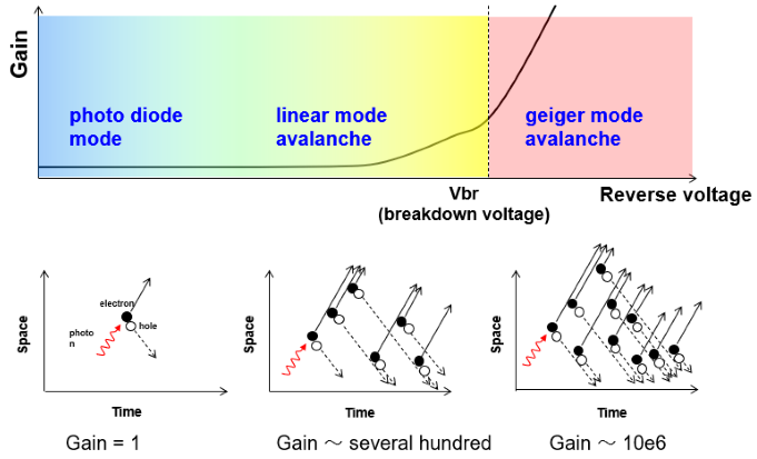
Figure 3. SPAD’s Geiger-mode operation. Image Credit: Hamamatsu Photonics Europe
To detect an additional incident photon, a quenching resistor must be included to suppress the current. Once enough gain and output signal amplitude have been reached, this prevents surges originating in the depletion region. When multiple SPAD channels are condensed into one output, an MPPC is produced.
In cases where several pixels fire simultaneously, the output becomes the cumulative sum of the standard pulses. In situations where more than one photon simultaneously incident on the same pixel, the signal presents as a 1 p.e. pulse as seen in Figure 4.
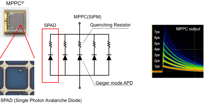
Figure 4. Unique MPPC structure and output. Image Credit: Hamamatsu Photonics Europe
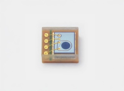
Hamamatsu's Si Avalanche Photodiode series S15415. Image Credit: Hamamatsu Photonics Europe
Si APD S15415 series
High-speed, compact Si APD that does not need temperature adjustments.
The S15415 series is a gain-stabilized APD (GS APD) with integrated temperature compensation built inside the sensor. This results in constant gain without the requirement of temperature adjustments. It is appropriate for laser monitors of optical rangefinders commonly used in an array of applications, from consumer to industrial.
Leading the Way in Photosensors for LiDAR
Hamamatsu Photonics has played an integral part in developing solutions for LiDAR in the automotive industry, providing a healthy portfolio of detectors and emitters for automotive and industrial LiDAR applications, including both APD and SiPM.
For example, Hamamatsu offers the distinctive Gain Stabilized Silicon Avalanche Photodiode (Si APD). The Si Avalanche Photodiode series S15415 boasts built-in temperature compensation functionality inside the chip. This guarantees constant gain with no requirement for temperature adjustments or a temperature-driven circuit.
Hamamatsu has also developed a new SIPM particularly for industrial applications. The key advantage of this product is the capability of operating at a very low breakdown voltage (25 V, total operating voltage below 50 V). The high number of SPAD channels also allows it to operate well in higher ambient light conditions.
Drawing from the incredible evolution of the photoelectric effect from technological cornerstone to scientific curiosity, the continual development of APD and SiPM technologies advances LiDAR-driven automation and safety while also paving the way to a future where intelligent systems, powered by these innovations, integrate seamlessly into everyday life.

This information has been sourced, reviewed and adapted from materials provided by Hamamatsu Photonics Europe
For more information on this source, please visit Hamamatsu Photonics Europe.