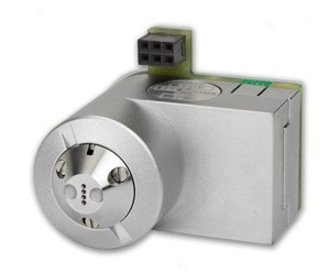
Filmetrics R-Series resistivity mapping tools combine KLA’s 45-year-old sheet resistance technology with benchtop instrument technology and a user interface honed over the previous 20 years by the Filmetrics team.
The 4PP contact four-point probe configuration is ideal for thin metal and ion implant layers, whereas the non-contact Eddy Current (EC) probe is preferred for thicker metal layers and soft or flexible conductive surfaces. These approaches enable a wide variety of measurements, including but not limited to the following:
- Sheet resistance
- Thin film thickness or resistivity
- Calculated thin film thickness and resistivity
- Calculate substrate resistivity
Using rectangular, linear, polar, and custom configurations, the Filmetrics R50 resistivity mapping system is designed to accommodate a wide variety of sample types with enhanced clearance and automated sample point mapping.
The R50 measurement performance is available in a light-tight enclosure with the KLA Instruments™ R54-Series systems, which also have the capacity to support automated X-Y-θ stages for full 200 mm or 300 mm wafer mapping of semiconductor and compound semiconductor wafers.
Models
Source: KLA Instruments™
| Model |
Sensor Type |
Measurement
Range |
Maximum
Map
Diameter |
XY Stage
Range |
Maximum
Sample
Height |
| R50-4PP |
Contact 4PP |
1 mΩ/sq -
200 MΩ/sq |
100 mm |
100 mm x
100 mm |
100 mm |
| R50-EC |
Non-contact
eddy current |
1 mΩ/sq -
50 Ω/sq |
100 mm |
100 mm x
100 mm |
100 mm |
| R50-200-4PP |
Contact 4PP |
1 mΩ/sq -
200 MΩ/sq |
200 mm |
200 mm
round |
100 mm |
| R50-200-EC |
Non-contact
eddy current |
1 mΩ/sq -
50 Ω/sq |
200 mm |
200 mm
round |
100 mm |
| R54-200-4PP |
Contact 4PP |
1 mΩ/sq -
200 MΩ/sq |
200 mm |
200 mm x
200 mm |
15 mm |
| R54-200-EC |
Non-contact
eddy current |
1 mΩ/sq -
50 Ω/sq |
200 mm |
200 mm x
200 mm |
15 mm |
| R54-300-4PP |
Contact 4PP |
1 mΩ/sq -
200 MΩ/sq |
300 mm |
300 mm
round* |
15 mm |
| R54-300-EC |
Non-contact
eddy current |
1 mΩ/sq -
50 Ω/sq |
300 mm |
300 mm
round* |
15 mm |
*Automated X-Y-θ stages
Common Optional Accessories

4PP-TypeA. Image Credit: KLA Instruments™
4PP-TypeB. Image Credit: KLA Instruments™

4PP-TypeC. Image Credit: KLA Instruments™
CondWafer-4PP. Image Credit: KLA Instruments™
Sheet Resistance and Other Measurement Applications
- Semiconductor wafer substrates
- Thin films (ITO, metals, TCOs, compound semiconductors)
- Solar Cells
- Metal foils
- Conductive rubbers & elastomers
- Glass substrates
- Conductive flexible substrates
- PCBs