Overview:
Our research group has discovered a new technique for compressing the computations of encryption and decryption operations known as Galois field arithmetic operations, and has succeeded in developing the world's most efficient Advanced Encryption Standard (AES) cryptographic processing circuit, whose energy consumption is reduced by more than 50% of the current level. With this achievement, it has become possible to include encryption technology in information and communication technology (ICT) devices that have tight energy constraints, greatly enhancing the safety of the next-generation Internet of Things (IoT). This result was announced on August 19, 2016 during the Conference on Cryptographic Hardware and Embedded Systems 2016 (CHES 2016) hosted by the International Association for Cryptologic Research (IACR) in Santa Barbara, USA.
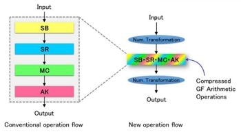 New Operation Compression Technology Based on Number Representation Transformation. (CREDIT: Naofumi Homma)
Social background of this development:
It is currently very common to exchange important personal or financial information over the Internet through ICT devices. Cryptographic techniques are used inside these devices to protect important information. In next-generation networks such as the IoT, which has attracted attention in recent years, it is expected that myriad devices will be connected to the network. Hence, it will be necessary to have built-in encryption technology in these connected devices to prevent malicious attacks. However, many battery or cell-driven devices with tight energy constraints are also included in the IoT and running energy-consuming encryption processes on these is a big challenge. One of the most widely used international standard encryption methods is AES. Since this is used in areas such as wireless LANs, it is very important for practical reasons to design energy-saving AES cryptographic processing.
History of this development:
Tohoku University and the NEC Corporation have been collaborating on research and development since 2013 with the purpose of improving the safety of ICT devices. In particular, they aim to build a system that will allow the new IoT services to be enjoyed with confidence. This will be done by developing technology that embeds encryption in small devices and sensors for the first time. This research and development is being carried out as part of the Grants-in-Aid for Scientific Research (KAKENHI) program No. 25240006 "Development of formal design technology for VLSI data path based on the Galois field computations." (Research representative: Naofumi HOMMA, Tohoku University).
Research details:
In the newly designed technique, the focus is on representing the AES encryption algorithm as a calculation based on a special numbering system called a Galois field. The research group has succeeded in transforming the input numerical representation into a different one, and is now able to perform multiple computations in one go. Using this method, the number of required circuit elements is reduced significantly. Furthermore, we have confirmed that the original output can be easily recovered by an inverse transformation. We have devised a computational method for inserting the transformed numerical representation and the inverse transformation before and after the computations, and for carrying out the computations internally using the transformed numerical representation. In addition, we have designed and developed an AES cryptographic processing circuit based on the new method and have confirmed that a single cycle can be carried out with less than half (about 45%) of the energy of the world's best circuit available so far. Both encryption and decryption can be carried out using this AES cryptographic circuit. It is ideally suited to global communication standards such as SSL and TLS.
Future plans:
Our plans now are to embed this cryptographic processing technique in actual systems, to carry out demonstration experiments, and to proceed further by applying the proposed method to other encryption algorithms. In addition, a configuration that is resistant to a variety of attacks will be considered with the aim of implementing it for practical use. Our future objective is to use this cryptographic processing technology to improve the safety of a whole variety of IoT ICT devices.