From the microchips in smartphones to the processors driving computers, semiconductor manufacturing underpins modern technology. One essential step that often goes unnoticed but is crucial to producing high-quality semiconductor devices is wafer inspection. This process, supported by cutting-edge wafer inspection sensors, ensures the reliability and performance of the final products.
In the early days of semiconductor manufacturing, inspection was predominantly a manual process, relying on human operators to identify defects on the surface of silicon wafers. As the demand for smaller and more powerful semiconductor devices grew, manual inspection proved insufficient and impractical due to human limitations in precision and speed.
The transition from manual inspection to automated, sensor-based approaches was a turning point in the semiconductor industry since the automated systems offered unmatched accuracy and efficiency, driving the evolution of wafer inspection technology. With the advent of these sensor-based systems, semiconductor manufacturers could meet the growing demand for smaller, more complex components and the need for rapid and precise quality control.
The Working Principles and Sensor Types
Sensor technology plays a pivotal role in detecting defects and ensuring the quality of semiconductor wafers. Wafer inspection sensors work on various principles, each suited to different inspection requirements. For instance, optical sensors utilize light to scan the surface of the wafers.
These sensors can help identify irregularities and defects by analyzing how light interacts with the wafer's surface. Similarly, Infrared sensors (IR sensors) take advantage of the radiation emitted by the wafer's surface by identifying variations in temperature caused by defects or contaminants, making them valuable in identifying subtle imperfections.
Laser scatter sensors are also used in defect detection when high precision is required for identifying even the tiniest defects. These sensors emit laser beams that interact with the wafer's surface, generating a scattering pattern that can reveal information about the wafer's surface, allowing for defect detection.
Challenges in Inspection
The semiconductor industry's quest for miniaturization poses significant challenges for wafer inspection. As semiconductor devices have shrunk, defects that were once relatively benign have become critical, potentially rendering an entire device useless, which urges the requirement for sensors with extraordinary sensitivity and precision. Moreover, with miniaturization, diffraction of light becomes a critical issue since diffraction limits the resolution of optical sensors, making it challenging to detect tiny defects. Researchers are continually working on improving optics and software algorithms to overcome these limitations.
When dealing with nanoscale features, subtle scattering effects can make defect identification difficult. Laser scatter sensors are crucial for overcoming these challenges, as they can capture detailed scattering patterns and identify defects that other sensors might miss.
Multiple layers and complex structures in modern semiconductor wafers can also lead to interference in the inspection process. Advanced sensors must be capable of distinguishing true defects from interference, ensuring accuracy and efficiency in the inspection process.
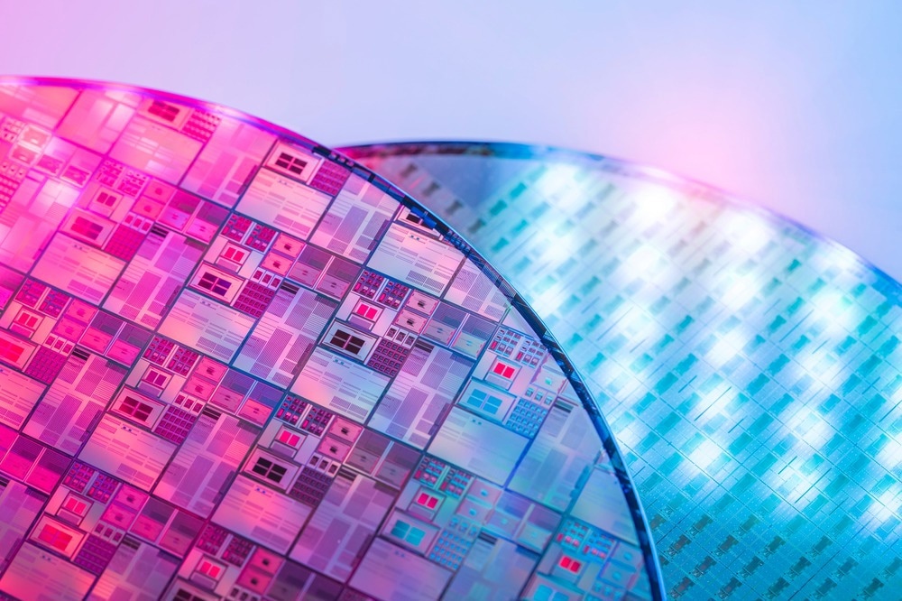
Image Credit: asharkyu/Shutterstock.com
Innovations in Sensor Technology
Some of the latest innovations in wafer inspection sensors include Machine Learning. Machine learning algorithms integrated into wafer inspection systems to enhance defect identification can learn from past inspection data and improve defect recognition capabilities over time, reducing false positives and negatives. Another notable innovation is improved optics via high-resolution imaging systems with advanced lenses and lighting techniques to overcome the challenges of diffraction and scattering.
Similarly, nondestructive testing (NDT) methods, such as terahertz imaging and X-ray microscopy, are becoming more prominent in wafer inspection, providing detailed information about the internal structure of wafers without damaging them and offering a more comprehensive view of potential defects.
Commercial Relevance of Wafer Inspection
In an industry where the cost of defects is measured in billions of dollars, efficient and effective wafer inspection is essential to reducing waste and ensuring product reliability. Companies that excel in wafer inspection stand to gain a competitive advantage.
One such company is KLA Corporation, a leader in process control solutions for semiconductor manufacturing. KLA's advanced wafer inspection systems, driven by cutting-edge sensor technology, play a vital role in enabling semiconductor manufacturers to produce high-quality components. These systems not only save manufacturers money by reducing defects and enhancing process efficiency but also contribute to the overall reliability of the electronic devices we rely on daily.
Conclusion
In conclusion, wafer inspection sensors have come a long way from the early days of manual inspection, and their evolution has been instrumental in meeting the industry's demand for smaller, more powerful devices. As semiconductor sizes continue to shrink, the challenges in inspection have grown, requiring innovations in sensor technology.
The economic implications of efficient wafer inspection are significant, with companies like KLA Corporation leading the way in this critical field. Looking to the future, we can expect further advancements in sensor technology driven by machine learning, advanced optics, and nondestructive testing methods, all of which will play a vital role in maintaining the high standards of the semiconductor industry and shaping tomorrow's digital landscape.
References and Further Reading
Adam, K., et al. (2018). Wafer quality inspection using memristive LSTM, ANN, DNN and HTM. In 2018 IEEE Electrical Design of Advanced Packaging and Systems Symposium (EDAPS) . IEEE, pp. 1-3. doi.org/10.1109/EDAPS.2018.8680907
Schurig, T., et al. (2017). Nondestructive wafer inspection utilizing SQUIDs. In Defect Recognition and Image Processing in Semiconductors 1997. Routledge, pp. 149-152. doi.org/10.1201/9781315140810-30
Wen, G., et al. (2020). A novel method based on deep convolutional neural networks for wafer semiconductor surface defect inspection. IEEE Transactions on Instrumentation and Measurement. doi.org/10.1109/TIM.2020.3007292
Zhu, J., et al. (2022). Optical wafer defect inspection at the 10 nm technology node and beyond. International Journal of Extreme Manufacturing. doi.org/10.1088/2631-7990/ac64d7
Disclaimer: The views expressed here are those of the author expressed in their private capacity and do not necessarily represent the views of AZoM.com Limited T/A AZoNetwork the owner and operator of this website. This disclaimer forms part of the Terms and conditions of use of this website.