As Moore’s Law predicted, the semiconductor manufacturing process continues to advance rapidly, with each new generation of technology reducing the size and spacing of features and layers on the integrated circuits (ICs).
Image Credit: Superior Sensor Technology
This greater density of circuitry on a wafer necessitates greater precision and an increasingly delicate and sophisticated fabrication process.
A number of the newer, more complex ICs today are comprised of a dozen or more layers produced in 300+ sequenced processing steps. Then, once the wafers have been fabricated, there is post-processing, succeeded by IC packaging and testing.
Below is a summary of some of the conventional steps in the IC manufacturing process:
- Wafer processing
- Cleaning of the silicon wafers
- Surface passivation
- Photolithography
- Etching
- Various depositions (chemical, atomic, physical)
- Wafer testing
- Die preparation
- Wafer mounting
- Wafer back grinding and polishing
- Wafer bonding and stacking
- Wafer bumping (if needed for flip chips)
- Through-silicon via (TSV) manufacture (if needed for 3D ICs)
- Die cutting
- IC packaging
- Die attachment to a substrate
- IC bonding (including wire bonding)
- IC encapsulation
- Laser marking and silkscreen printing
- IC testing
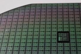
Figure 1. Image of Silicon Wafer with Etched Circuitry. Image Credit: Superior Sensor Technology
Today, the manufacturing of semiconductors places exceptionally high demands on pressure measurement technology to guarantee a high-quality process. All fabrication steps, including cleaning, etching and polishing, must be extra precise as the finished product uniformity is measured in microns.
Consequently, testing and inspection are conducted to measure variances during all aspects of semiconductor manufacturing.
The Role of Pressure Sensors in Semiconductor Manufacturing
Pressure sensors are utilized throughout IC manufacturing to conduct real-time pressure measurements throughout the different stages of the semiconductor process. Some of the common uses include:
- Enhancing the precision and control of the wafer polishing heads through the constant application of pressure. In chemical mechanical polishing (CMP) systems, measurements such as parallelism of the polishing heads and characterization is a critical part of the fabrication process.
- Ensuring consistent wafer cleaning by verifying how effective the wafer polishing head is. If the polishing head is not conditioned properly, or it is lacking a uniform roughness on its surface, the removal of external particles will not be effective. Any particle residue may mean that ICs fail inspection and test.
- Limiting the number of cracked or unbounded wafers. As mentioned, CMP is a key manufacturing process for semiconductors, as enhancing uniformity throughout the polishing process is crucial. An uneven polishing head can cause cracks to appear in the wafer, resulting in ICs being discarded.
- Verify die-to-substrate planarization, particularly for flip-chip bonding. Uniform pressure is needed to prevent die cracking or open electrical connections. As with wafer cracking, an IC with a damaged die or open electrical connection cannot be used.
- Discerning wear on plates and other parts could lead to wafer bonding errors. In order to apply level amounts of pressure through the attachment process, the plates must be even. However, like other components, they are subject to wear over time which may result in them becoming uneven. By determining the pressure variations, the equipment can identify the problem and sound a repair alarm before faulty parts are assembled.
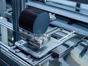
Figure 2. Image of Wafers in Fabrication. Image Credit: Superior Sensor Technology
Superior Sensor’s NimbleSenseTM Architecture for Semiconductor Manufacturing
With an extremely low noise floor, the NimbleSense architecture is ideal for the precise pressure measurements that are demanded by semiconductor equipment to enhance long-term stability, optimize accuracy and boost overall IC production yields.
However, the benefits of NimbleSense extend well beyond the low noise floor. Some of its application-specific building blocks offer extra value add for semiconductor manufacturing.
Multi-Range TechnologyTM
Multi-Range technology means that just one pressure sensor is able to operate at maximum performance over numerous pressure ranges. As wafer lots possess various numbers of layers, and bonding/packaging can differ, the pressure requirements will vary.
Multi-Range allows one sensor to be adjusted without any degradation in performance to meet the pressure demands for different fabrication processes.
Advanced Digital Filtering
Semiconductor manufacturing demands precision, and external factors, including noise from air conditioning or other equipment, building vibrations, etc., can severely influence the accuracy of pressure sensors.
Utilizing Superior’s integrated advanced digital filtering technology, these pressure sensors cancel out the noise these factors create before they reach the sensor sub-system. Thus, the noise is removed before it becomes an error signal that can generate inaccurate readings.
Conclusion
Semiconductor manufacturing is advancing at a rapid pace, with each new generation of technology reducing the size and spacing of features and layers on ICs.
This increased density of circuitry on a wafer places extremely high demands on pressure measurement technology to guarantee a high-quality process. Each step in the fabrication process must be executed to the highest degree of accuracy as the finished product uniformity is measured in microns.
Superior Sensor’s specialized pressure sensor technology, predicated on proprietary NimbleSense architecture, offers a number of benefits for semiconductor equipment, including exceptional long-term stability, greater accuracy, state-of-the-art digital filtering and Multi-Range technology.
To learn more about the NimbleSense architecture, visit Superior’s technology page, or contact Superior Sensor to discuss a semiconductor-related project.

This information has been sourced, reviewed and adapted from materials provided by Superior Sensor Technology.
For more information on this source, please visit Superior Sensor Technology.