As a result, optimizing the reaction sites for carrier transfer and concentration is critical to achieving low-temperature functioning.
Two-dimensional semiconductors, particularly transition metal dichalcogenides (TMDs) such as MoS2, WSe2, and SnSe2, have been considered for use as active sensing materials. Several issues remain, however, including irreversible sensing behavior, sluggish reaction and recovery time, and high oxidation rate at high working temperatures.
To increase sensing properties at low temperatures, a nanostructure with a wide effective reaction area (i.e., specific surface, crystal defects, etc.) and optimized carrier concentration is extremely preferred.
Heterostructures composed of 2D semiconducting TMDs and metal oxide semiconductors have recently been studied as possible active sensing materials for chemiresistive gas sensors.
The effective charge concentration can be adjusted by charge transfer between the two atomic layers due to their differing electronic band structures. These materials offer a high specific surface area and a quick reaction time.
Researchers analyzed the gas sensing properties of a 1D–2D hybrid network structure containing SnO2 nanowires and SnSe2 layers. After selenization, the hybridized nanowire networks demonstrated improved chemisorption of oxygen ions and stable NO2 detection capability at ambient temperature. The study was published in the journal iScience.
Results and Discussion
A vapor-liquid-solid (VLS) approach was used to make pristine SnO2 nanowires, which were then selenized utilizing a CVD-based direct selenization procedure, as seen in Figure 1A.
First, interdigitated Au (3 nm)/Pt (300 nm)/Ti (50 nm) electrodes with a 20 μm width and spacing were fabricated, and then SnO2 nanowires were selectively grown at 900 °C for 30 minutes using the VLS growth technique.
Using Se powder as the Se precursor, the ultrathin SnSe2 was produced on the surface of the SnO2 nanowires network at 550 °C for 30 minutes.
The Au layer was employed to selectively develop SnO2 nanowires, resulting in a network topology of SnO2 nanowires growing on the interdigitated electrodes. This networked structure of SnO2 nanowires is retained following the CVD-based selenization process, as seen in Figure 1B.
Low and high magnification field emission scanning electron microscopy (FESEM) images of the 1D SnO2–2D SnSe2 hybrid nanowire network are shown in Figures 1C and 1D. Highly dense nanowires with a diameter of 40 to 50 nm are orientated randomly.
A field emission transmission electron microscopy (FETEM) picture of the 1D SnO2–2D SnSe2 hybrid nanowire network is shown in Figure 1E. On the surface of grown SnO2 nanowires, an ultrathin SnSe2 layer with a thickness of a few nanometers was created evenly.
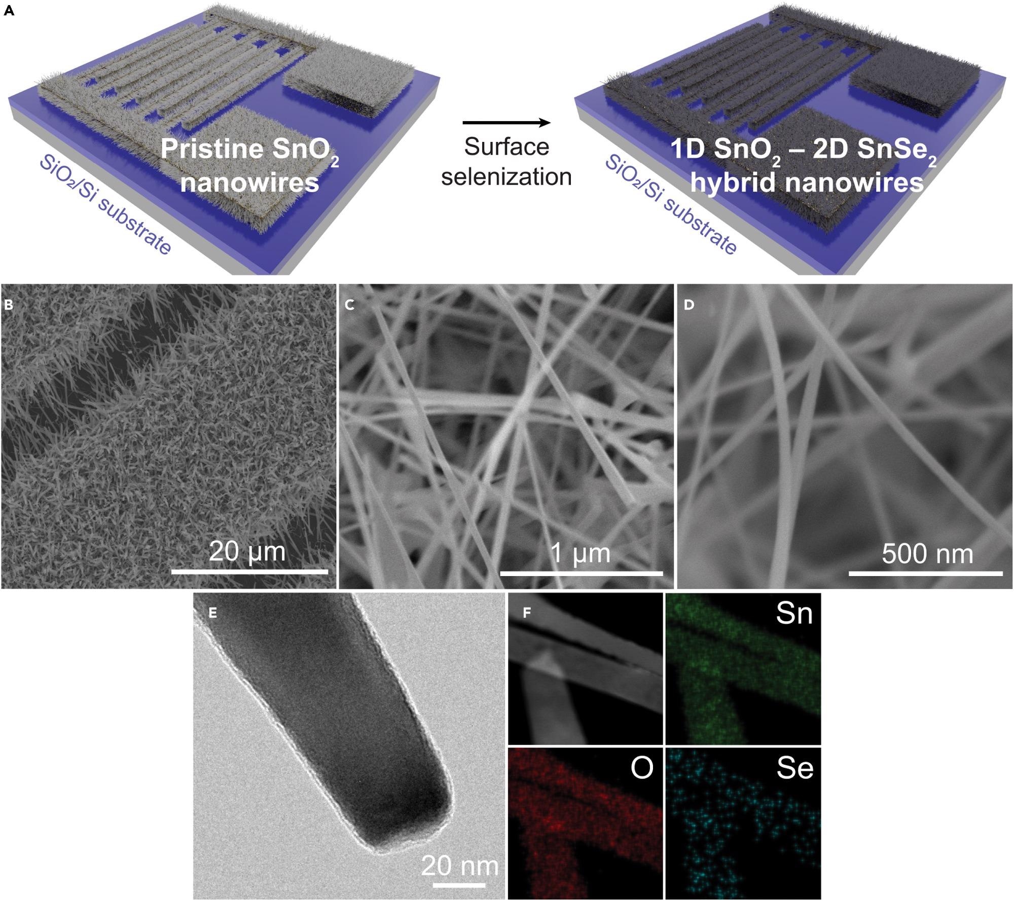
Figure 1. Preparation and structural characterization of 1D SnO2–2D SnSe2 hybrid nanowire network(A) Illustration showing the CVD-based selenization process of pristine SnO2 nanowires.(B) FESEM image of 1D SnO2–2D SnSe2 nanowire network selectively grown on Au/Pt/Ti interdigitated electrodes.(C and D) FESEM images of SnO2 nanowires with ultrathin SnSe2 under (C) low and (D) high magnification.(E) FETEM image of SnO2 nanowire after the selenization process showing ultrathin shell of SnSe2 formed on SnO2 nanowire.(F) STEM-HAADF image with corresponding EDS mapping images of Sn (green), O (red), and Se (blue). Image Credit: Seo, et al., 2022
X-ray diffraction (XRD) was used to analyze the crystal structure of the SnO2-SnSe2 hybrid nanowires. The (002), (011), (003), and (110) planes of SnSe2 are attributed to the peaks at roughly 29.6°, 30.6°, 43.5°, and 47.5°, respectively.
The XRD spectra of as-grown SnO2 nanowires before and after CVD-based surface selenization are shown in Figure 2A. This implies that the ultrathin SnSe2 nanowire networks were effectively produced on the surface of SnO2.
Raman spectroscopy of virgin SnO2 nanowires reveals three distinct peaks at 474, 633, and 776 cm-1, respectively.
The in-plane A1g and out-of-plane Eg modes are attributed to the Raman peaks, respectively. The few scattering centers in the few-layered SnSe2 are responsible for the Eg mode’s low intensity. The frequency of these two distinctive Raman peaks is determined by the number of SnSe2 layers present.
As a consequence, crystalline SnSe2 is well produced on the surface of SnO2 nanowires with less than 5 layers, as shown by FETEM in Figure 1E and XRD findings.
SnO2’s in-plane A1g vibrational mode similarly has a low peak intensity, implying the presence of SnO2 nanowires under the selenized surface. However, the A1g mode has shifted from 633 to 631 cm-1, indicating that oxygen has been incorporated into the crystal lattice.
This can alter the planar lattice’s interaction, influencing the in-plane vibrational mode. Furthermore, a modest Raman peak of about 107 cm-1 is found, which correlates to the B3g form of SnSe. This suggests that the as-prepared nanowires have a partly selenized area.
The valence state of every element on the surface of the selenized SnO2 nanowires was further studied using X-ray photoelectron spectroscopy (XPS), as illustrated in Figures 2C–E.
Sn-O bonding in SnO2 (Sn 3d5/2: 487.19 eV, Sn 3d3/2: 495.6 eV) and Sn-Se bonding in SnSe2 (Sn 3d5/2: 485.63 eV, Sn 3d3/2: 494.16 eV) are seen in the high-resolution Sn 3d spectrum in Figure 2C.
The occurrence of the ultrathin SnSe2 layer on the surface of SnO2 nanowires is indicated by the modest intensity of the Sn-Se bonding peaks.
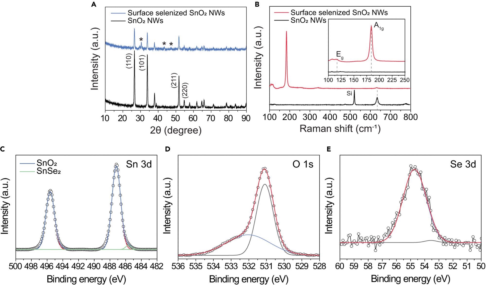
Figure 2. Structural and chemical characterizations of 1D SnO2–2D SnSe2 hybrid nanowire network (A) XRD spectra of pristine SnO2 nanowire (top) and SnO2 nanowires with ultrathin SnSe2 (bottom). (B) Raman spectra of SnO2 nanowires before (top) and after (bottom) selenization process. The inset shows the magnified Raman spectra in the range of 100–250 cm−1, in which two characteristic Raman peaks of 2D SnSe2 indicate the successful formation of ultrathin SnSe2 layer on the surface of the SnO2 nanowires. (C–E) XPS spectra of (C) Sn 3d, (D) O 1s, and (E) Se 3d for the1D SnO2–2D SnSe2 heterostructure. Image Credit: Seo, et al., 2022
Based on these findings, it can be inferred that the CVD procedure properly selenized the surface of the rutile SnO2 nanowires with ultra-thin SnSe2 with excellent crystallinity. The development of a 2D SnSe2 layer on the surface of 1D SnO2 nano-wires boosts the interface with the environment, which should improve gas sensing capability.
Figure 3A shows a schematic illustration of the 1D SnO2 nanowire–2D SnSe2-based gas sensor. The dynamic resistance responses of the SnO2 nanowires were examined before and after the surface selenization at varying NO2 concentrations and temperatures to study the characteristics of the ultrathin 2D SnSe2 layers on 1D SnO2 nanowires.
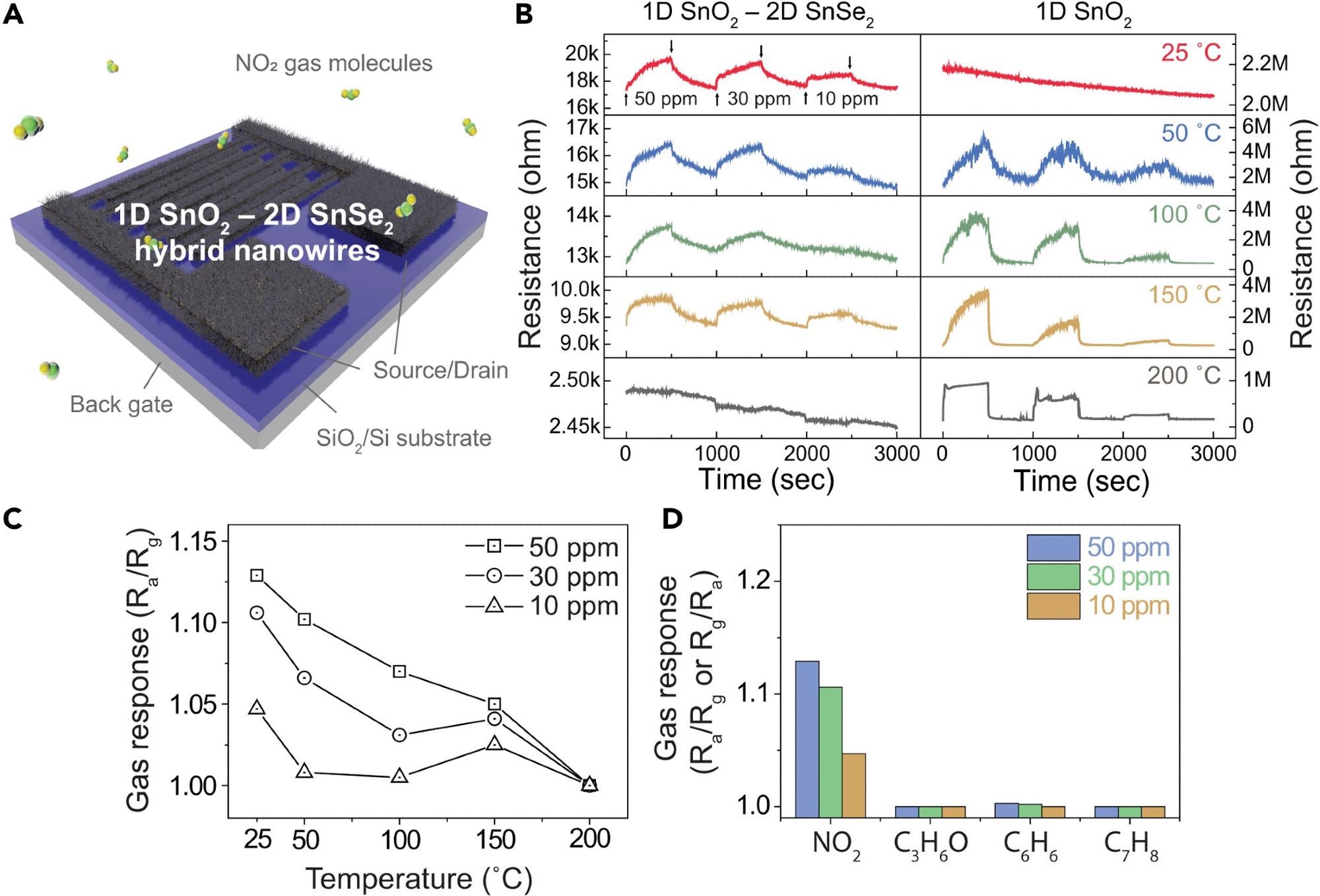
Figure 3. Gas sensing characteristics of 1D SnO2–2D SnSe2 hybrid nanowire network-based gas sensor forNO2 gas(A) Illustration of NO2 gas sensor based on SnO2 nanowires with ultrathin SnSe2.(B) Dynamic resistance curves of pristine SnO2 nanowires (right) and 1D SnO2–2D SnSe2 heterostructure (left)-based gas sensor to different NO2 gas concentrations of 10–50 ppm at different temperatures (room temperature – 200 °C).(C) Comparative analysis of NO2 gas sensitivity at different operating temperatures and gas concentrations of 10–50 ppm.(D) Comparison of gas sensing response of the 1D SnO2 nanowire–2D SnSe2 heterostructure-based gas sensor against various gases (NO2,C3H6O, C6H6,and C7H8) at different gas concentration from 10 to 50 ppm. Image Credit: Seo, et al., 2022
At ambient temperature, a hybrid gas sensor based on a network of 1D SnO2 and 2D SnSe2 nanowires demonstrated acceptable responsiveness, although resistance dropped as temperature increased.
The sensor’s sensitivity is related to the gas concentration and decreases as the temperature rises. The buildup of electrons transmitted from the as-prepared SnO2 nanowires on the surface of the SnSe2 layer improves the sensing capabilities at ambient temperature.
At room temperature, the ultrathin SnSe2 layer on SnO2 nanowire networks greatly improved gas sensing capability. Due to the higher concentration of chemisorbed oxygen ions, the reactions between NO2 molecules and adsorbed oxygen ions proliferate, resulting in a better gas response.
By testing the detecting behavior in various gases at ambient temperature, the selectivity of the 1D SnO2–2D SnSe2 heterostructure-based gas sensor was examined. The sensor features NO2 gas selectivity.
Stimulating adsorbed oxygen molecules and lattice ionic oxygen to create active O2-, O-, and mobile O2- species determines the pace of chemical processes. This effect lasts until the operational temperature reaches a particular point.
Furthermore, the exothermic gas molecule is difficult to adsorb by thermal energy, and the gas molecules are rapidly desorbed, lowering the gas response.
At ambient temperature, ultrathin SnSe2 layers atop SnO2 nanowire networks greatly improved gas sensing capability.
Even at low NO2 concentrations, a 1D SnO2 nanowire–2D SnSe2 heterostructure-based gas sensor for NO2 gas demonstrates good responsiveness. The back-gate bias reduces the energy barrier and increases gas sensing.
These findings show that the reaction to SNO2/Sgas is nearly equal to the response to NO2, showing that the 2D SnSe2-based gas sensor possesses NO2 selectivity.
The energy gap between the Fermi level of metal oxide and the valence band of the gas molecule determines the usual gas molecule adsorption systems on the surface of the sensing material.
At room temperature, the transient resistance to various NO2 concentrations was measured when gate bias (Vg = 0.5, 1.5, and 2.5 V) was applied. Even at the lowest NO2 concentration, the gas sensor provides a very good reaction (more than 50% greater) compared to the response without gate voltage.
The gate voltage enhanced the responsiveness and recovery behavior, as demonstrated in Figure 4B (1.5 V). The recovery time was reduced from 373 seconds to 346 seconds, while the response time was reduced from 375 s to 110 s, using a gate voltage of 1.5 V.
This means that the back-gate voltage lowers the energy barrier for adsorption on reactive sites, resulting in a more efficient interaction between NO2 gas molecules and the nanowire surface at ambient temperature.
However, the recovery period was still lethargic, necessitating more study to enhance it.
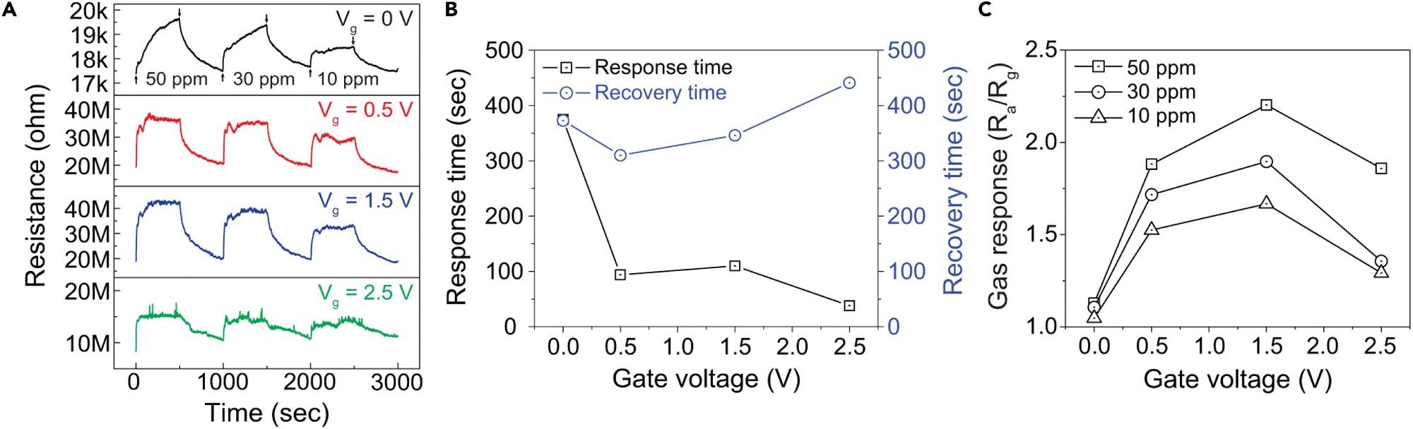
Figure 4. Enhancement in gas sensing performance of 1D SnO2–2D SnSe2 heterostructure-based gas sensor for NO2 gas by introducing the back-gate bias (A) Gate-bias dependent dynamic resistance curves of the 1D SnO2–2D SnSe2 hybrid nanowire networks-based gas sensor to different NO2 gas concentrations of 10–50 ppm at room temperature. Electrical characteristics measured with VDS=1 V and Vg= 0, 0.5, 1.0, 1.5, 2.0, 2.5 V.(B) Response and recovery times as a function of the gate voltage under the exposure to 50 ppm of NO2 gas at room temperature.(C) Comparison of NO2 gas sensing response at different back-gate bias and gas concentrations of 10–50 ppm. Image Credit: Seo, et al., 2022
At room temperature, Figure 4C shows the reaction to various NO2 gas concentrations as a function of back-gate bias. At ambient temperature, the best gas reaction was 2.2 (Ra/Rg) when exposed to 50 ppm NO2 gas at Vg = 1.5 V.
This result was nearly twice as high as the gas response of 1.13 (Ra/Rg) when the gate bias was not applied. With rising gas concentration, the response also increased, which might be due to the increased number of reactive gas molecules.
The energy barrier for the adsorption of analyte gas molecules on the surface of 1D–2D hybrid nanowires is controlled by the back-gate voltage, which contributes to electron flow.
As a result of using the back-gate voltage, the sensing performance was increased.
Conclusion
A 1D–2D hybrid nanowire network made up of SnSe2 layers and SnO2 nanowires were used to create a gas sensor. The gas sensor showed enhanced sensing performance, including reaction time and sensitivity, when back-gate bias (Vg = 1.5 V) was applied.
The energy barrier for NO2 gas adsorption on the reactive sites was reduced by the back-gate voltage, resulting in improved sensing performance. Compared to a previous sensor that works at room temperature, the sensor displayed improved gas detection qualities for NO2 gas at ambient temperature.
The findings might lead to improvements in sensing performance for low-temperature gas sensors, nanostructure design, and a variety of applications for future sensing platforms, such as portable diagnostic tools and smart sensing devices.
Journal Reference:
Seo, J., Nam, S. H., Lee, M., Kim, J.-Y., Kim, S. G., Park, C., Seo, D.-W., Kim, Y. L., Kim, S. S., Kim, U. J., and Hahm, M. G. (2022) Gate-controlled gas sensor utilizing 1D–2D hybrid nanowires network. iScience. 25, 103660 Available Online: https://www.sciencedirect.com/science/article/pii/S2589004221016308
References and Further Reading
- Ahn, M. W., et al. (2009) On-chip fabrication of ZnO-nanowire gas sensor with high gas sensitivity. Sensors Actuators B Chemical, 138, pp. 168–173. doi.org/10.1016/j.snb.2009.02.008.
- An, B., et al. (2020) Controlled synthesis of few-layer SnSe2 by chemical vapor deposition. RSC Advances, 10, pp. 42157–42163. doi.org/10.1039/d0ra08360g.
- Camargo Moreira, O. L., et al. (2019) High selectivity gas sensing and charge transfer of SnSe2. ACS Sensors, 4, pp. 2546–2552. doi.org/10.1021/acssensors.9b01461.
- Cao, A., et al. (2014) Silicon nanowire-based devices for gas-phase sensing. Sensors, 14, pp. 245-271. doi.org/10.3390/s140100245.
- Chen, H., et al. (2017) Visible-light excited strong red emission of SnO2 nanostructures. Materials Research Express, 4, p. 045019. doi.org/10.1088/2053-1591/aa6bbd.
- Cheng, J. P., et al. (2016) A review of recent developments in tin dioxide composites for gas sensing application. Industrial & Engineering Chemistry Research, 44, pp. 1–22. doi.org/10.1016/j.jiec.2016.08.008.
- Cho, B., et al. (2015) Jeong Charge-transfer-based gas sensing using atomic-layer MoS2. Scientific Reports, 5, pp. 1–6. doi.org/10.1038/srep08052.
- Cho, B., et al. (2016) Two-dimensional atomic-layered alloy junctions for high-performance wearable chemical sensor. ACS Applied Materials & Interfaces, 8, pp. 19635–19642. doi.org/10.1021/acsami.6b05943.
- Choi, Y. J., et al. (2008) Novel fabrication of an SnO2 nanowire gas sensor with high sensitivity. Nanotechnology, 19, p. 095508. doi.org/10.1088/0957-4484/19/9/095508.
- Choi, S. Y., et al. (2017) Effect of Nb doping on chemical sensing performance of two-dimensional layered MoSe2. ACS Applied Materials & Interfaces, 9, pp. 3817–3823. doi.org/10.1021/acsami.6b14551.
- Costa, I. M., et al. (2018) Sb doping of VLS synthesized SnO2 nanowires probed by Raman and XPS spectroscopy. Chemical Physics Letters, 695, pp. 125–130, doi.org/10.1016/j.cplett.2018.02.014.
- Cui, H., et al. (2020) Tellurene nanoflake-based NO2 sensors with superior sensitivity and a sub-parts-per-billion detection limit. ACS Applied Materials & Interfaces, 12, pp. 47704–47713. doi.org/10.1021/acsami.0c15964.
- Dey, A (2018) Semiconductor metal oxide gas sensors: a review. Materials Science and Engineering B, 229, pp. 206–217. doi.org/10.1016/j.mseb.2017.12.036.
- Donarelli, M & Ottaviano, L (2018) 2D materials for gas sensing applications: a review on graphene oxide, MoS2, WS2 and phosphorene. Sensors, 18, p. 3638. doi.org/10.3390/s18113638.
- Feng, P., et al. (2014) Gas sensors based on semiconducting nanowire field-effect transistors. Sensors, 14, pp. 17406–17429. doi.org/10.3390/s140917406.
- Gonzalez, J M & Oleynik, I I (2016) Layer-dependent properties of SnS2 and SnSe2 two-dimensional materials. Physics Review B, 94, p. 125443. doi.org/10.1103/PhysRevB.94.125443.
- Gu, D., et al. (2017) Enhanced NO2 sensing of SnO2/SnS2 heterojunction based sensor. Sensors Actuators B, 244, pp. 67–76. doi.org/10.1016/j.snb.2016.12.125.
- Han, Y., et al. (2018) Design of hetero-nanostructures on MoS2 nanosheets to boost NO2 room-temperature sensing. ACS Applied Materials & Interfaces, 10, pp. 22640–22649. doi.org/10.1021/acsami.8b05811.
- Hao, J., et al. (2018) Hierarchical SnS2/SnO2nanoheterojunctions with increased active-sites and charge transfer for ultrasensitive NO2 detection. Nanoscale, 10, pp. 7210–7217. doi.org/10.1039/c8nr01379a.
- Hellmich, W., et al. (1997) Field-effect-induced gas sensitivity changes in metal oxides. Sensors Actuators B, 43, pp. 132–139. doi.org/10.1016/S0925-4005(97)00195-0.
- Henning, A., et al. (2015) Electrostatic limit of detection of nanowire-based sensors. Small, 11, pp. 4931–4937. doi.org/10.1002/smll.201500566.
- Jiang, J., et al. (2017) Two-step fabrication of single-layer rectangular SnSe flakes. 2D Materials, 4, p. 021026. doi.org/10.1088/2053-1583/aa6aec.
- Kang, M. J., et al. (2019) Atomic-layered tungsten diselenide-based porous 3D architecturing for highly sensitive chemical sensors. Physica Status Solidi, 13, p. 1900340. doi.org/10.1002/pssr.201900340.
- Khan, M. A. H., et al. (2021) Back-gate GaN nanowire-based FET device for enhancing gas selectivity at room temperature. Sensors, 21, p. 624. doi.org/10.3390/s21020624.
- Kolmakov, A., et al. (2005) Enhanced gas sensing by individual SnO2 nanowires and nanobelts functionalized with Pd catalyst particles. Nano Letters, 5, pp. 667–673. doi.org/10.1021/nl050082v.
- Kumar, R., et al. (2020) MoS2-based nanomaterials for room-temperature gas sensors. Advanced Materials Technologies, 5, p. 1901062. doi.org/10.1002/admt.201901062.
- Lee, E., et al. (2018) Two-dimensional transition metal dichalcogenides and metal oxide hybrids for gas sensing. ACS Sensors, 3, pp. 2045–2060. doi.org/10.1021/acssensors.8b01077.
- Li, H., et al. (2012) Fabrication of single-and multilayer MoS2 film-based field-effect transistors for sensing NO at room temperature. Small, 8, pp. 63–67. doi.org/10.1002/smll.201101016.
- Li, R., et al. (2017) SnO2/SnS2 nanotubes for flexible room-temperature NH3 gas sensors. RSC Advances, 7, pp. 52503–52509. doi.org/10.1039/c7ra10537a.
- Liu, W., et al. (2021) AuPt Bimetal-Functionalized SnSe2 microflower-based sensors for detecting sub-ppm NO2 at low temperatures. ACS Applied Materials & Interfaces, 13, pp. 20336–20348. doi.org/10.1021/acsami.1c02500.
- Li, X., et al. (2020) Layered SnSe2 microflakes and SnSe2/SnO2 heterojunctions for low-temperature chemiresistive-type gas sensing. Journal of Materials Chemistry C, 8, pp. 15804–15815. doi.org/10.1039/d0tc02589e.
- Lu, D., et al. (2021) Phase controllable synthesis of SnSe and SnSe2 films with tunable photoresponse properties. Applied Surface Science, 541, p. 148615. doi.org/10.1016/j.apsusc.2020.148615.
- Matysiak, W., et al. (2020) Synthesis of hybrid amorphous/crystalline SnO2 1D nanostructures: investigation of morphology, structure, and optical properties. Science Reports, 10, pp. 1–10. doi.org/10.1038/s41598-020-71383-2.
- McAlpine, M. C., et al. (2007) Highly ordered nanowire arrays on plastic substrates for ultrasensitive flexible chemical sensors. Nature Materials, 6, pp. 379–384. doi.org/10.1038/nmat1891.
- Moumen, A., et al. (2021) Robust room-temperature NO2 sensors from exfoliated 2D few-layered CVD-grown bulk tungsten di-selenide (2H-WSe2). ACS Applied Materials & Interfaces, 13, pp. 4316–4329. doi.org/10.1021/acsami.0c17924.
- Paolucci, V., et al. (2020) Self-assembled SnO2/SnSe2 heterostructures: a suitable platform for ultrasensitive NO2 and H2 sensing. ACS Applied Materials & Interfaces, 12, pp. 34362–34369. doi.org/10.1021/acsami.0c07901.
- Ping, J., et al., (2017) Recent advances in sensing applications of two-dimensional transition metal dichalcogenide nanosheets and their composites. Advanced Functional Materials, 27, p. 1605817. doi.org/10.1002/adfm.201605817.
- Rai, R. K., et al. (2019) Morphology controlled synthesis of low bandgap SnSe2 with high photodetectivity. Nanoscale, 11, pp. 870–877. doi.org/10.1039/c8nr08138g.
- Ricciardella, F., et al. (2017) Effects of graphene defects on gas sensing properties towards NO2 detection. Nanoscale, 9, pp. 6085–6093. doi.org/10.1039/c7nr01120b.
- Shalev, G (2017) The electrostatically formed nanowire: a novel platform for gas-sensing applications. Sensors (Basel), 17. doi.org/10.3390/s17030471.
- Shao, X., et al. (2018) Flaky nano-crystalline SnSe2 thin films for photoelectrochemical current generation. RSC Advances, 8, pp. 32157–32163. doi.org/10.1039/c8ra04639e.
- Shehada, N., et al (2015) Ultrasensitive silicon nanowire for real-world gas sensing: noninvasive diagnosis of cancer from breath volatolome. Nano Letters, 15, pp. 1288–1295. doi.org/10.1021/nl504482t.
- Sun, Y. F., et al. (2012) Metal oxide nanostructures and their gas sensing properties: a review. Sensors, 12, pp. 2610–2631. doi.org/10.3390/s120302610.
- Thang, N. T., et al. (2020) Controlled synthesis of ultrathin MoS2 nanoflowers for highly enhanced NO2 sensing at room temperature. RSC Advances, 10, pp. 12759–12771. doi.org/10.1039/D0RA00121J.
- Vemula, M., et al. (2021) Hybrid 2D/0D SnSe2-SnO2 vertical junction based high performance broadband photodetector. Journal of Alloys and Compounds, 883, p. 160826. doi.org/10.1016/j.jallcom.2021.160826.
- Wang, C., et al. (2010) Metal oxide gas sensors: sensitivity and influencing factors. Sensors, 10, pp. 2088–2106. doi.org/10.3390/s100302088.
- Wang, T., et al. (2021) Boosted interfacial charge transfer in SnO2/SnSe2 heterostructures: toward ultrasensitive room-temperature H2S detection. Inorganic Chemistry Frontiers, 8, pp. 2068–2077. doi.org/10.1039/d0qi01326a.
- Yan, W., et al. (2020) Enhanced NO2 sensitivity in Schottky-contacted n-type SnS2 gas sensors. ACS Applied Materials & Interfaces, 12, pp. 26746–26754. doi.org/10.1021/acsami.0c07193.
- Yan, W., et al. (2018) Effects of ambient humidity and temperature on the NO2 sensing characteristics of WS2/graphene aerogel. Applied Surface Science, 450, pp. 372–379. doi.org/10.1016/j.apsusc.2018.04.185.
- Zhao, S., et al. (2018) Highly enhanced response of MoS2/porous silicon nanowire heterojunctions to NO2 at room temperature. RSC Advances, 8, pp. 11070–11077. doi.org/10.1039/c7ra13484c.
- Zhang, Y., et al. (2018) Synthesis and surface-enhanced Raman scattering of ultrathin SnSe2 nanoflakes by chemical vapor deposition. Nanomaterials, 8, p. 515. doi.org/10.3390/nano8070515.
- Zhang, D., et al. (2017) Room-temperature SO2 gas-sensing properties based on a metal-doped MoS2 nanoflower: an experimental and density functional theory investigation. Journal of Materials Chemistry A, 5, pp. 20666–20677. doi.org/10.1039/C7TA07001B.
- Zhou, X., et al. (2015) Ultrathin SnSe2 flakes grown by chemical vapor deposition for high-performance photodetectors. Advances Materials, 27, pp. 8035–8041. doi.org/10.1002/adma.201503873.