May 13 2015
Analog Devices, Inc. today introduced a FET input AFE with an integrated ADC driver designed to interface directly with current mode sensors such as photo diodes and high output impedance voltage sensors.
 Integrated Analog Front-end Simplifies Sensor Interfaces (Graphic: Business Wire)
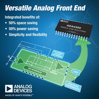
The ADA4350 integrates a FET input amplifier, switching network and ADC driver into a single package, which simplifies design and lowers power and PCB footprint by more than 50 percent compared to discrete implementations.
The ADA4350 features low-noise performance at low frequencies of 90nV/√Hz at 10 Hz and broadband noise of 5 nV/√Hz at 100 kHz to maximize the signal-to-noise ratio of the sensor output. Wide dynamic range measurement for small, sensitive signals such as photons or electrons is enabled with the inclusion of integrated gain switching. The on-chip programmability of the ADA4350 allows designers to select external, optimized feedback components. With one chip, a single-ended or differential sensor current or voltage signal can be transformed to a high-speed, low-noise, single-ended or differential-output voltage.
In analytical measurement applications, light may need to be monitored over many decades of intensity. This requires a variety of gain switching networks that often incorporate multiple external amplifiers and analog switches, which increases the potential for system errors. The ADA4350 integrates the switching networks and input amplifier to minimize leakage and allow the switching network to select up to six externally configurable feedback networks. In test and measurement systems, the same high measurement accuracy must be maintained across the gain levels as the user adjusts the input range of the instrument. For measuring a wider dynamic range, the ADA4350 is an ideal choice because of its high-impedance/low-Ib input amplifier and serial port-controlled switch network. The device also reduces PCB footprint while significantly increasing channel count without thermal density restrictions.